Hello Horu5,
If I may suggest, it would be a good idea to buy yourself an simple transistor tester from somewhere like Ebay and/or look through the various threads on this sites forums about transistor testing and matching - it will make your testing simpler and less expensive")
When it comes to matching transistors, there are two parameters to look at: the current gain (hfe) and the device's Vbe voltage. A decent transistor tester will help you measure both. Most people match on the hfe: I would try and aim to match this within 2 to 5% depending upon the application.
The Class A amplifier web site
The Class-A Amplifier Site
is a wealth of information that would help you in building a JLH amplifier, including transistor selection.
Hope this helps
Mike
If I may suggest, it would be a good idea to buy yourself an simple transistor tester from somewhere like Ebay and/or look through the various threads on this sites forums about transistor testing and matching - it will make your testing simpler and less expensive
When it comes to matching transistors, there are two parameters to look at: the current gain (hfe) and the device's Vbe voltage. A decent transistor tester will help you measure both. Most people match on the hfe: I would try and aim to match this within 2 to 5% depending upon the application.
The Class A amplifier web site
The Class-A Amplifier Site
is a wealth of information that would help you in building a JLH amplifier, including transistor selection.
Hope this helps
Mike
Hi John and Rallyfinnen,
thanks for your suggestions of the simulation file I posted. I have tried them against the orginal circuit and posted them in the enclosed attachment which also contains the .asc files and models. The Excel file shows which asc file is what.
I changed each model's value to R1 to get the Emitter current to about 2 Amps and tweaked the R13 value to get the output DC offset as close to zer as I could.
I found that switching the 0.1 resistors from the PNP Emitter to their respective Collector ajoining their BD139 had a detrimental effect of the THD measured, increasing the distortion by a factor of 7 at lower powers and about 3 at higher powers. How it would sound I obviously have no idea?
Increasing the values of the resistor in the Collector circuit only helped marginally.
The bootstrap mod had a slightly detrimental effect as the table shows.
Other points: I used the BD139C model in the simulation as it was the first one I came accross - I think it was in Bob Cordell's collection.
The use of a 4KHz input frequency is a hang over from me learning from the excellent set of lessons in the Construction/software set of threads on this site. Having got one sim working well, I basically modified it for new models as they came along - a hangover from my engineering and coding days
This modelling exercise has been a great help for me in learning LTSpice and I welcome suggestions on modifications to try out - so thanks.
I am off to the 'states in a few weeks and aim to raid my reclamation sources over there for genuine devices so I can build a simple amp based on the simulation - good stuff for a summer evening as I have mentioned before. If it sounds better, then maybe I'll update my current JLH amp. So if folks have better models/transistors etc. please add to the knowledge for us all.
Kind regards
Mike
Attachments
Hello Horu5,
If I may suggest, it would be a good idea to buy yourself an simple transistor tester from somewhere like Ebay and/or look through the various threads on this sites forums about transistor testing and matching - it will make your testing simpler and less expensive
When it comes to matching transistors, there are two parameters to look at: the current gain (hfe) and the device's Vbe voltage. A decent transistor tester will help you measure both. Most people match on the hfe: I would try and aim to match this within 2 to 5% depending upon the application.
The Class A amplifier web site
The Class-A Amplifier Site
is a wealth of information that would help you in building a JLH amplifier, including transistor selection.
Hope this helps
Mike
Hello Fred, thanks for your Reply! I bought a transistor tester and tested, and got out hfe=58. which I considered to low after studiing the Datasheet of the MJ15003. So I thought about a more real testing with 10V and aound 1A and 85°C and got very different results.
results:
MJ15003 (Digikey) measured with 10V PSU: 25°C -> hfe=70, 85°C -> hfe=113;
MJ15003 (Digikey) measured with Tester: 25°C -> hfe=58, 85°C -> hfe=90
2N3055 (used, from chinese Kit) measured with 10V PSU: 25°C -> hfe 131, 85°C -> hfe=125
2N3055 (used, from chinese Kit) measured with Tester: 25°C -> hfe 175, 85°C -> hfe=304
Probably this tester (Type: Transistor Tester TFT -> picture) isn't strong enough for power transistors. ..

Last edited:
Hi again,
Sorry, I was thinking of testing the small signal devices and did not answer your question.
You are quite correct in that the hfe will vary with the Collector current and the method you have tried is valid for power transistors. However, you will have to be very careful in how long you test a free standing device (i.e. not on a heatsink) with a current of 1 Amp going through it and 10Volts across it with no protection.
This may help further.
hFE Tester for NPN Power Transistors
Kind regards
Mike
Last edited:
fredbloggstwo:
Hope you update us when you build it!
Are you planning to leave room for the RC on the PCB? I was thinking about it last night, and I remember having stability problems related to the area around the base of the upper output transistor when trying fast outputs together with ccs (JLH96). I'm guessing the lower impedance from the RC would improve stability too.
I also remember reading something about stability problems and paralleled CFP/S-pair, however I'm not sure if it applies to class A? Maybe it's related to the switching with (low bias) push/pull?
Yes.
To get the most power and efficiency upper an lower outputs should both share the work equally. In the 69 version the resistors to the upper base can be adjusted to tune this. This will affect the distortion too. This is what I have been playing around with trying to minimize distortion on the 69 amps, in combination with finding the Iq where the output transistors are happiest (most linear region I guess).
In the 96 version with ccs, they seem to share the currents nicely, but in Mikes version with CCS & CFP outputs (that was discussed above), there was something odd with the current sharing between upper and lower transistors.
I doubt the time delay matters? Not as bad as class AB where there is a dead period.
Most simple class A signal amplifers use a collector output current source connected to an emitter connected unity gain current amplifier. Instinctively that seems better. Is the low output impedance of the JLH feedback alone? What would happen if the current sink was swapped to a non modulated current source using PNP. 5 watts target power.
Most simple class A signal amplifers use a collector output current source connected to an emitter connected unity gain current amplifier. Instinctively that seems better. Is the low output impedance of the JLH feedback alone? What would happen if the current sink was swapped to a non modulated current source using PNP. 5 watts target power.
I mentioned that I intended to try an unusual phono preamp. The 75 uS the 160R coil resistance of the Denon DL 110 shunted with 470 nF. The inductance isn't high enough to interfere. The 3180/318 uS is fairly conventional except a massive gain of 100 meaning 1000 at 20 Hz. The eq is Riaa and not IEC. The sound is the absolute opposite of distorted although measurements might say differently. The op amp MC33078 and NE5532 tried. The 33078 sounds more open and less processed. 5532 very acceptable. I have some LM833 I could try. The single 10nf polystyrene capacitor doing these eqs. Much as I respect the NAD 3020 phono stage it's not good enough. suspect a first class design made with low grade capacitors to blame.
I calculated the same idea for the AT95 and got nowhere.. The 470nF is a 63v polyester. That would be something to do a little better. Some ancient Pink Floyd sounding excellent. I use a 1M input loading. This shows 200 mV input offset when OK. If 12V trouble and a dead cartridge or a bad risk. The very high loading means only the 75uS is being asked to improve the slew rate limiting. For a phono stage that matters
The turntable is Garrard 401. Arm Hadcock GH 220 or 9 inch..A Shure weight crca 5g added for the 8 cu compliance. If not the resonant frequency is about 13 Hz which to me sounds wrong. The effect is more open sound when 10 Hz. 2g playing weight. The Hadcock is very quirky.
Very much a JLH turntable. Lenco gl75 almost as good. I imagine John had one of these on a TD150.
@rallyfinnen - your 2.2k position is not where I think it needs to be. I suggest it should be between Q7 collector and the centre (output) rail. To balance the one in the lower half.
You can leave the emitter resistors in the MJ15004's but I'd still recommend putting current sharers in the emitter/collector positions of Q1/Q10 etc.
You can leave the emitter resistors in the MJ15004's but I'd still recommend putting current sharers in the emitter/collector positions of Q1/Q10 etc.
Only just caught up with the developments!
Fredbloggs2 mod 5 is what I had in mind.
How does it look in the sims?
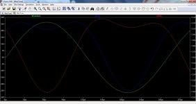
I tried that one first, but the currents still looked strange. Here is a plot of mod5 upper and lower currents together with output voltage. They look ok on low levels, but get odd with higher output.
Again, I'm not sure how the current sharing matters, but I guess it could have some effect on the PS etc.
Attachments
This is the same problem I had when I designed my variant a while back. The only way I could get the currents to equalise was to increase the local feedback, which the 2.2k base and local emitter resistors provide.
It can be forced to balance by increasing this local feedback. This means by reducing the 2.2k or increasing the emitter resistors or both,.
First, though, I would suggest that using local emitter resistors is always to be recommended when parallelling devices to improve current sharing.
Increasing the local feedback by introducing the 2.2k in the upper stage or reducing its value in both halves will have a detrimental effect on distortion, because the nonlinear emitter-base voltages then have to be applied to the resistor. So what was a minimal offset current is then larger.
One further option you might look at which should preserve the low distortion is to keep the "local" emitter resistors to ensure current sharing. Then instead of connecting the 2.2k resistors from the base to ground on the lower half, or base to centre in the upper, try replacing these by four 8.2k resistors each one tied locally between the base and emitter of the drivers. This should provide a balanced drive impedance while not incurring the excess non-linear component.
It won't however provide local feedback, only balance the impedances.
Another point I found was that the reduction in current in one half at higher currents was due to gain roll-off in the output transistors. That means perhaps the Iq is set too high. If your expected output is 36V into 6 ohms, say, the peak (nominal) current would be 6A, suggesting an Iq of perhaps 4A, or 1A in each device. Or maybe trying a sim with MJ21193 which have a more linear gain than the 15004, though they cost more and seem to be getting even more so.
... and I see, the BD139C is a Cordell model, not an actual device. Should have guessed.
And regarding distortion, I also found that when the currents are more symmetrical, the distortion is minimised. Seems that the symmetry is needed to cancel even harmonics. So the use of local feedback and optimum Iq was my solution.
In your case I'm not sure if the asymmetry will be eliminated by my repositioned base resistors, as there will still be gain roll-off even in the CFP - this can only reflect, after all , the combined gains of the two devices. Hence my suggestion for the more linear gain device.
Last edited:
And one more thing ...
The impedance of R7 is a problem (too low) as the input impedance to Q4 is high (two E-B junctions in series, one from Q4 the other from Q1,Q13 etc.)
I was going to suggest connecting it to the emitter of a driver when the current sharing resistors are included, but I've now run a sim and that increases 3rd harmonic!.
In general it will reduce the gain and my preference would be to make it ten times higher and connect to a low voltage supply rail (generated from a voltage doubler on the PSU), (with a reverse bias protection diode on Q4 to the main negative rail) or you could use a current mirror fed with a dummy current from the ground rail. Anything to increase the impedance.
So it seems OK as it is even with emitter resistors in Q1/Q13 etc added.
Last edited:
Here is your problem:
In the original circuit, the two output transistors had an Iq set by the driver/VAS stage current. This had to be approximately half the required peak base current at peak output. Just over, in fact, due to the gain roll-off at high currents.
In your circuit the CFP have a high current gain. Say the MJ15004 has a gain of 60 at 2A and that will require a base current of 33mA. At 33mA the gain of the BD139 is about 100. So it needs only 330uA. As mentioned before, the pair will have a high current gain roll-off due to the MJ15004, in the main. That would suggest setting the pre-driver stage current to only 660uA. To low, really, for a high power amp although it is not having to drive a Miller capacitor, so it seems possible.
To equalise the currents, then local feedback needs to be significantly higher to increase the effective base currents. If the current gain of the MJ15004 is 120 at 1A* the driver has to swing about +25mA, -5mA. So to balance, the local currents probably need to be at least 100mA. That would mean using a VAS stage current of maybe 1.5mA, and a base resistor causing a current shift of about 1mA for a 1A output swing. That means, say, using a 1k base resistor and 1 ohm current sharing resistors.
But the overall distortion will increase because you will have lost some gain.
As a starting point, I used 0.68 ohm current sharing resistors, a 1k base to ground/centre rail load resistor and 4mA in the VAS stage driver, with adjustments to the input bias current to re-zero the output rail.
Distortion was higher - 0.1% instead of 0.01%, but no sign of asymmetrical currents in the output transistors. The quiescent current stability would be higher IMO and easier to set.
I leave it to you to optimise the performance!
* edit- I use this as an illustration. The current gain probably won't alter this much.
John (Ellis),
Here is the LT model for the BD139, perhaps you could help us all by including it and making changes to one of the .asc files, such as components, adjusting the Iq and DC offset etc, so we can all see what you are trying to explain.
Kind regards
Mike
Here is the LT model for the BD139, perhaps you could help us all by including it and making changes to one of the .asc files, such as components, adjusting the Iq and DC offset etc, so we can all see what you are trying to explain.
Kind regards
Mike
Attachments
Mike/Rally
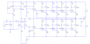
I haven't got round to learning LT spice in any depth. Here is my sim pic- hope you can make the adjustments in LT Spice yourselves.
It is basically Mike's Mod 5. I've used BD139/BD140 in the VAS stage as I did not have the models for the devices you used - maybe I should copy them from the previous posts.
I've taken the lower base resistor of (your) Q4 to a -23 V extra rail which in practice means -62V but that can be obtained with a voltage doubler on the - rail.
John Linsley Hood made an astute choice of feedback and grounding resistors. The stability of the circuit may well depend on the low gain due to the 220 grounding resistor, limiting the input stage gain to 5mA/V. While the different bias on the 6.8k (now 68k) resistor goes a long way to reducing the increased distortion due to the local feedback, making the feedbadk resistor 1.2k and 100 reduces it further.
But the stability is lost and a 22pF compensation capacitor is needed across the feedback resistor. Not checked stability margin etc - over to you!
- Home
- Amplifiers
- Solid State
- JLH 10 Watt class A amplifier