I had stability issues with the helpers that made me discount them reasonably quickly. I've hit my goals with the diodes plus the 47K resistor, and that seems to be a reasonably straightforward approach.
I'm working now on building more of an amp around this, so am interested in PSRR and such issues. The main supplies I'm thinking of using, XP Power EML30's, specify 200mV pk-pk ripple. I threw a 100mV pk 7KHz source in series with one of the main supplies in simulation and saw it was suppressed to -115dBV (95dB PSRR), so not really quite what I need to push it into the noise floor.
Separating the supply for the LatFETs and everything else helps immeasurably here. If I power everything but the LatFET drains from a clean +/-45V supply, and put my 100mV 7KHz tone on the 36V LatFET supply, It's suppressed to -150dBV (130dB PSRR), plenty.
So the supply for the second-stage diffamp and VAS really has to be regulated. A simple LM317L/LM337L reg has >40dB ripple rejection up to 20KHz, so that'll do nicely for the role, pushing 100mV pk noise on the +45V supply down to -155dBV.
I've further split out the input diffamp and it's cascode, using a low noise +/-15V supply, based on the TI TPS7A49. This reg provides >52dB rejection at audio frequencies, so we should be down now to -167dBV (147dB PSRR).
In short, I'm confident of being able to use this amp with switching supplies, with unmeasurable ripple & noise contribution, as long as I use post-regulation for the low current VAS and input stages.
Here's the schematic of my sim now:
The LT1028 on the front end is for testing clipping response. By powering this from our +/-15V supply, and setting it up with X4 gain, then dividing by four to go into the power amp input, the LT1028's clipping response (which is really lovely if the simulation is to be believed) then defines the response for the whole amp.
So here's where I am with the Protel schematic of the "signal PCB" (everything but the LatFETs and power supplies):
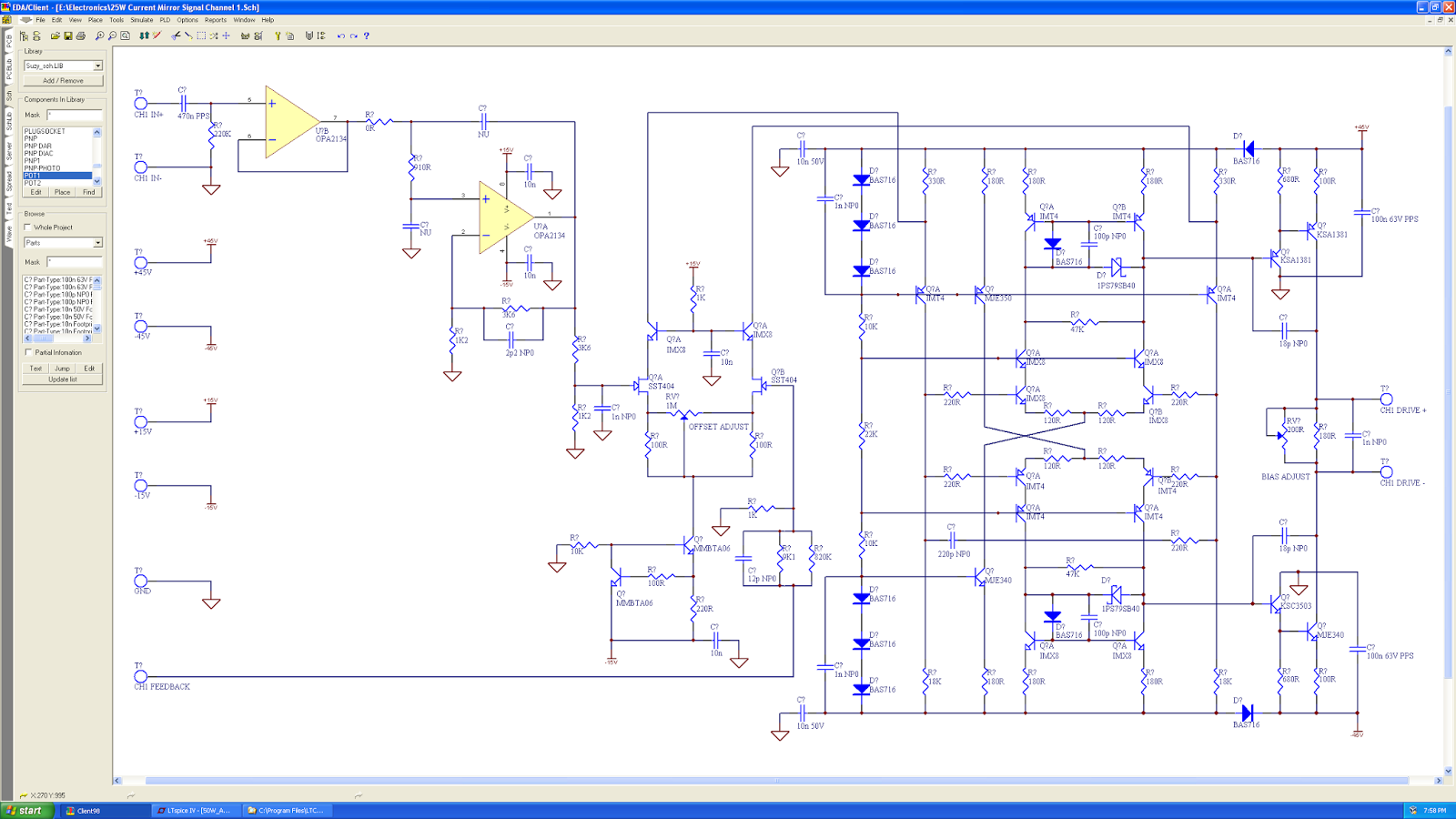
I've made use of the input opamp to implement a sallen-key 2-pole low-pass. The other channel gets a high-pass. They don't have to be used (just leave out some components and insert zero-ohm links to defeat them), but should I wish I can use the PCB to build a two-way active crossover power amp, rather than the more usual stereo amp.
I'm working now on building more of an amp around this, so am interested in PSRR and such issues. The main supplies I'm thinking of using, XP Power EML30's, specify 200mV pk-pk ripple. I threw a 100mV pk 7KHz source in series with one of the main supplies in simulation and saw it was suppressed to -115dBV (95dB PSRR), so not really quite what I need to push it into the noise floor.
Separating the supply for the LatFETs and everything else helps immeasurably here. If I power everything but the LatFET drains from a clean +/-45V supply, and put my 100mV 7KHz tone on the 36V LatFET supply, It's suppressed to -150dBV (130dB PSRR), plenty.
So the supply for the second-stage diffamp and VAS really has to be regulated. A simple LM317L/LM337L reg has >40dB ripple rejection up to 20KHz, so that'll do nicely for the role, pushing 100mV pk noise on the +45V supply down to -155dBV.
I've further split out the input diffamp and it's cascode, using a low noise +/-15V supply, based on the TI TPS7A49. This reg provides >52dB rejection at audio frequencies, so we should be down now to -167dBV (147dB PSRR).
In short, I'm confident of being able to use this amp with switching supplies, with unmeasurable ripple & noise contribution, as long as I use post-regulation for the low current VAS and input stages.
Here's the schematic of my sim now:
The LT1028 on the front end is for testing clipping response. By powering this from our +/-15V supply, and setting it up with X4 gain, then dividing by four to go into the power amp input, the LT1028's clipping response (which is really lovely if the simulation is to be believed) then defines the response for the whole amp.
So here's where I am with the Protel schematic of the "signal PCB" (everything but the LatFETs and power supplies):
I've made use of the input opamp to implement a sallen-key 2-pole low-pass. The other channel gets a high-pass. They don't have to be used (just leave out some components and insert zero-ohm links to defeat them), but should I wish I can use the PCB to build a two-way active crossover power amp, rather than the more usual stereo amp.
Last edited:
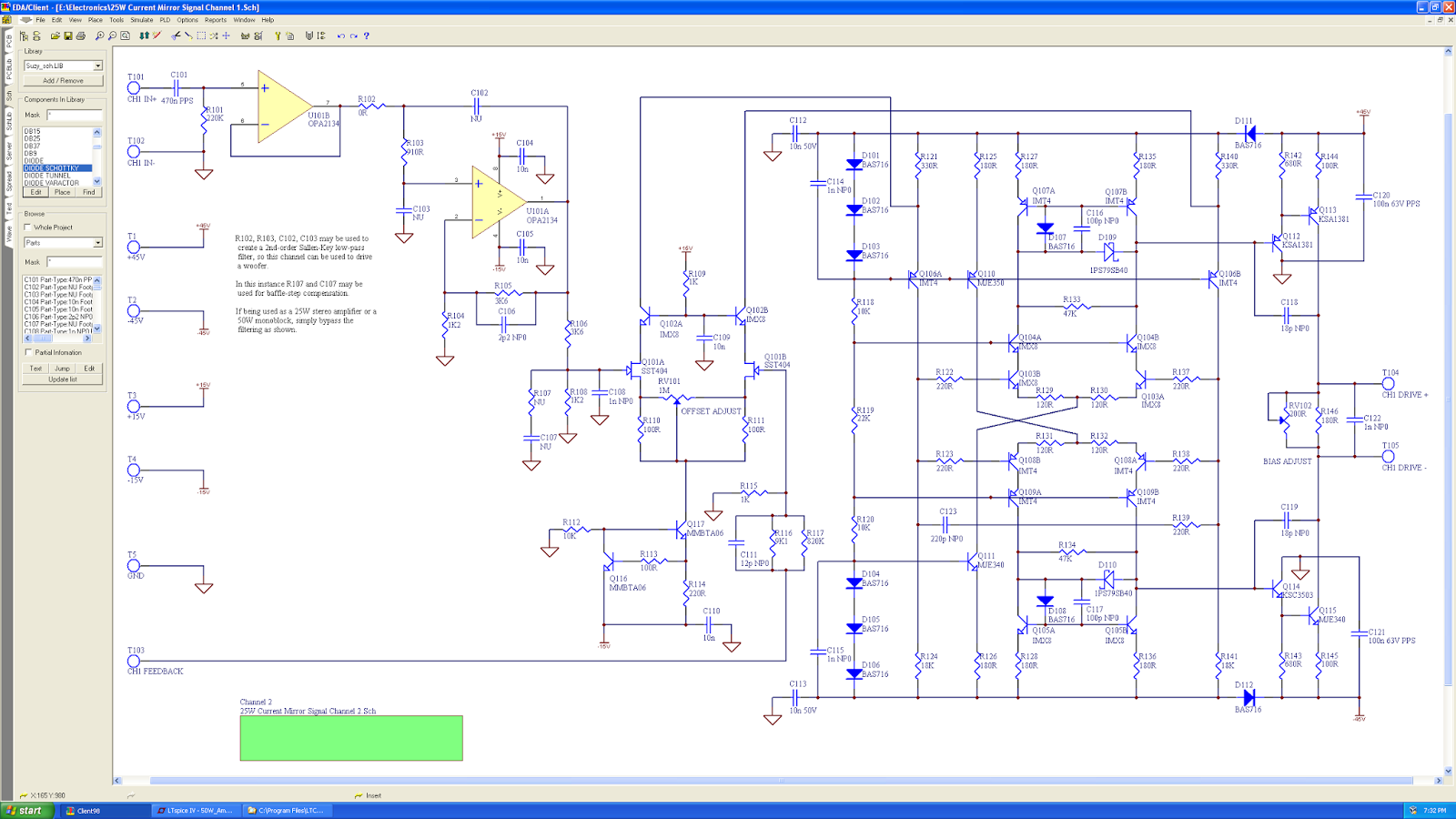
"Final" version of schematics for the low power board:
Channel 1:
Channel 2:
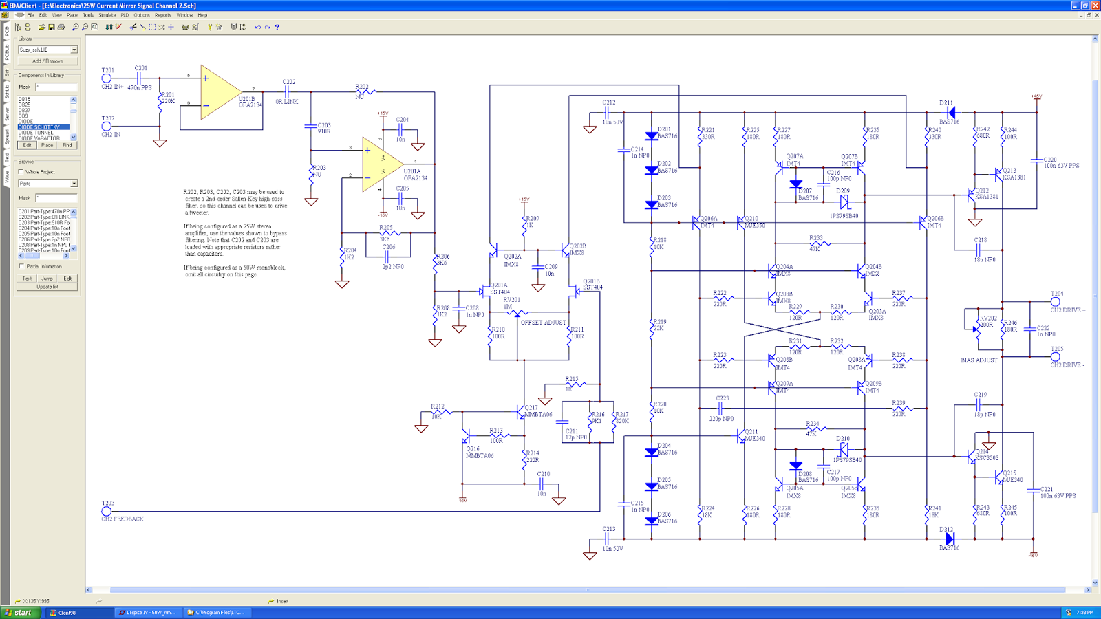
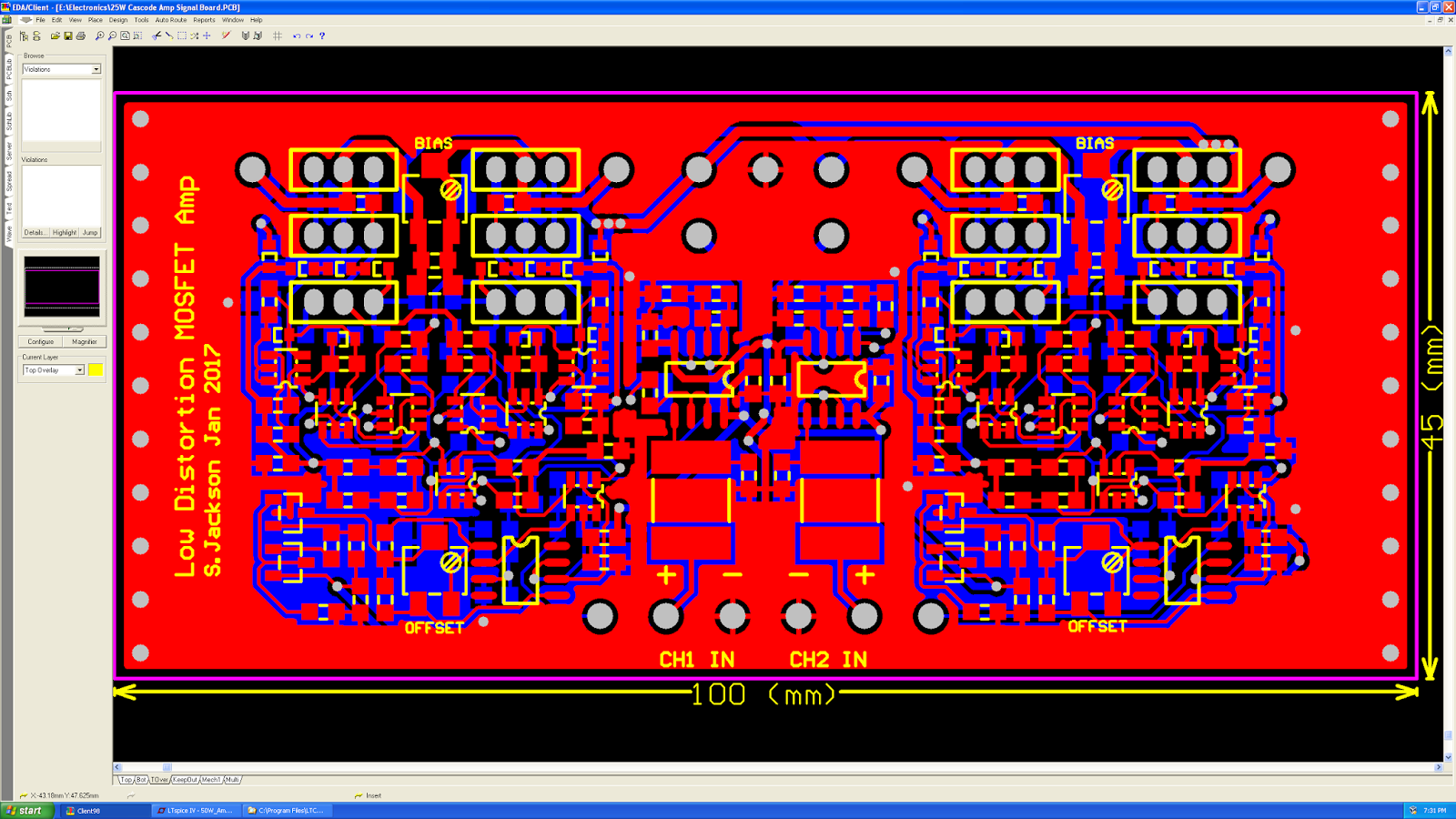
PCB layout is nice and compact. Despite using SOT-26 (6 pin SOT-23) and 0201 MELFs, (or 0805 flat resistors), as well as SOD-523 diodes, it still works nicely at 10 mil track and spacing with two layers, so nothing terribly advanced. I've gone for 30 mil tracks across the VAS (with 0402 MELFs), 15 mil power traces, and 10 mil for everything else. PCB ended up 100x45. The Hammond 1455 case dictates the 100mm width. The only through-hole parts are the TO-126 VAS transistors and the MJE340/350 current source/sink.
Top layer:
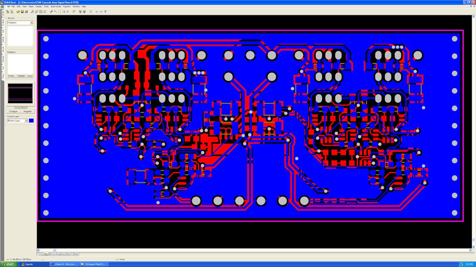
Bottom layer:
Channel 1:
Channel 2:
PCB layout is nice and compact. Despite using SOT-26 (6 pin SOT-23) and 0201 MELFs, (or 0805 flat resistors), as well as SOD-523 diodes, it still works nicely at 10 mil track and spacing with two layers, so nothing terribly advanced. I've gone for 30 mil tracks across the VAS (with 0402 MELFs), 15 mil power traces, and 10 mil for everything else. PCB ended up 100x45. The Hammond 1455 case dictates the 100mm width. The only through-hole parts are the TO-126 VAS transistors and the MJE340/350 current source/sink.
Top layer:
Bottom layer:
I bet those MJE340/350 through holes really bug you 😉 If so, look up MJD340/350 - same die, DPAK casing 😉
Hi SuzyjI had stability issues...
Do you have plots of Loop Gain to check stability?
Presumably the extra amp section would reduce stability, I am curious to learn how it works out in your circuit.
Best wishes
David
Loop open (substituting 90000K for 9K feedback resistor):
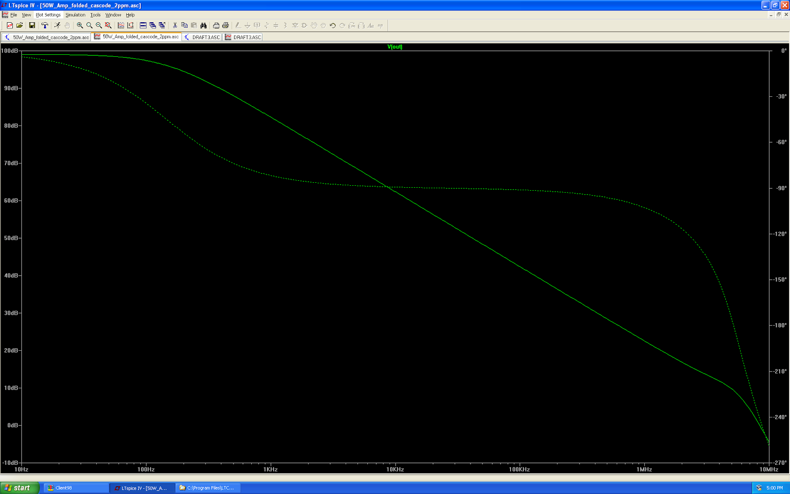
I reckon that's about 70 degrees phase margin at 20dB gain. I've still got 45 degrees at 13.2dB gain, so I'm slightly overcompensated 🙂
Loop closed (20dB gain):
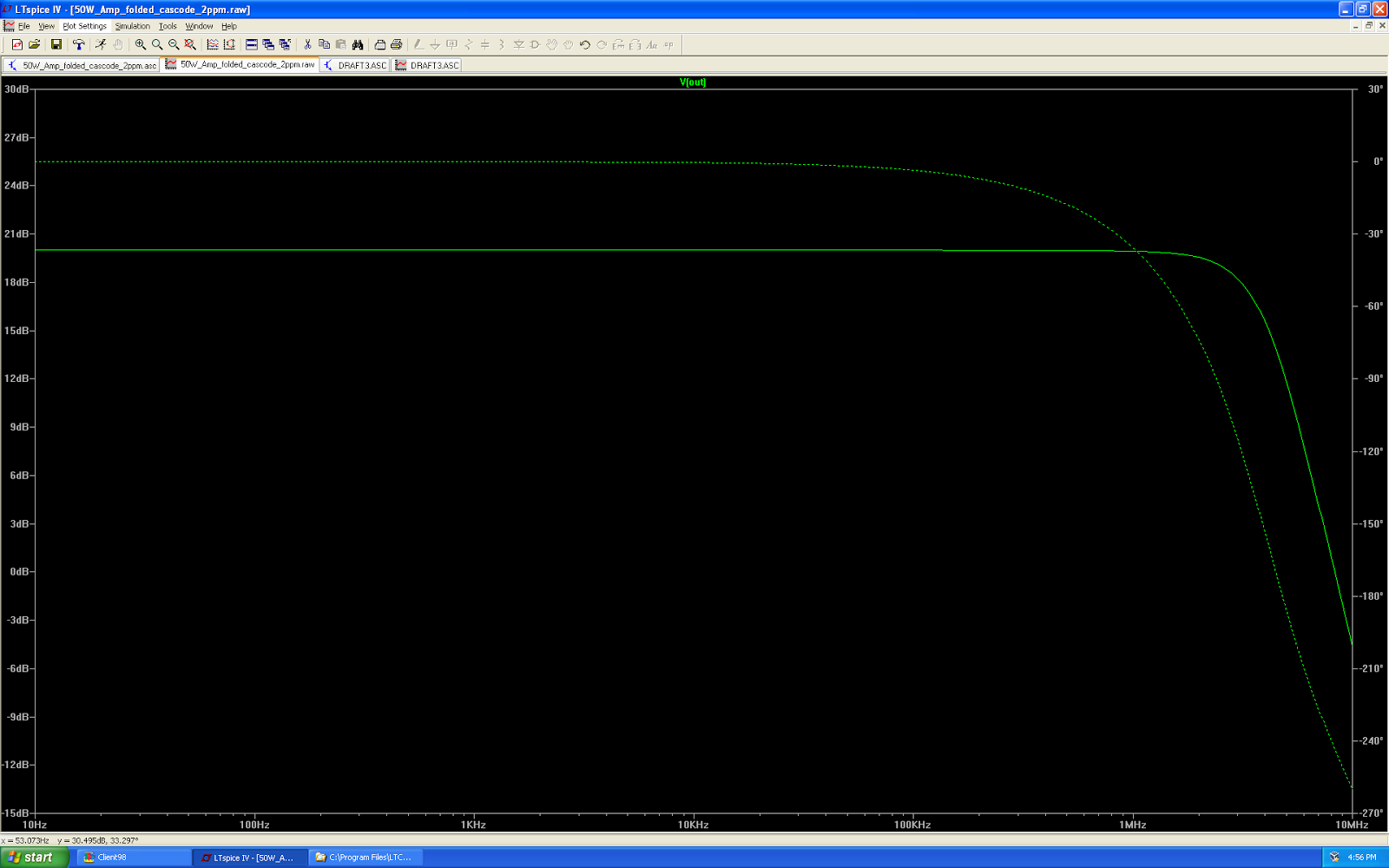
-3dB point is at 3.5 MHz. 🙂
It was actually quite straightforward to stabilise, at least in simulation. Certainly no more tricky than the usual AEM6000.
I reckon that's about 70 degrees phase margin at 20dB gain. I've still got 45 degrees at 13.2dB gain, so I'm slightly overcompensated 🙂
Loop closed (20dB gain):
-3dB point is at 3.5 MHz. 🙂
It was actually quite straightforward to stabilise, at least in simulation. Certainly no more tricky than the usual AEM6000.
Last edited:
The "Loop closed" plot appears to be identical to the "Loop open" plot, do I misread it?
You haven't used a Tian probe to look more closely at the stability?
Best wishes
David
OK, you made an edit as I wrote my post, some confusion.
It looks that what you have shown is not the loop gain.
You haven't used a Tian probe to look more closely at the stability?
Best wishes
David
OK, you made an edit as I wrote my post, some confusion.
It looks that what you have shown is not the loop gain.
Last edited:
The "closed loop" plot appears to be identical to the "open loop" plot, do I misread it?
You haven't used a Tian probe to look more closely at the stability?
Best wishes
David
Typo - fixed now.
I confess I have no idea what a Tian probe - I shall google.
My usual method for reading phase margin is to do a transient sim with 0V input, play with the first stage degeneration resistor values to get the DC offset down to 1nV or so, then open the loop up by substituting a >10Meg resistor. Then I do an ac sim and have a look at the frequency where the gain drops to my operating gain, and check what the phase is at this point. Phase margin is just 180-the phase reading at that point.
Not sure what the Tian probe gives me that I don't already have.
Not sure what the Tian probe gives me that I don't already have.
My usual method...
Not really a reliable method and not that informative, hence the Tian probe.
It is pretty standard for "advanced" amps that aspire to push the limits.
Even Tian isn't quite completely accurate, there's a helpful discussion on Frank Wiedmann's website, he was the one who actually wrote the LTspice implementation.
Best wishes
David
Ah, okay, I see. From Weidmann's page:
This is why I spend some time nulling the offset first. 1nV offset closed loopwith 120dB additional gain ends up 1mV, so still properly linear, and increasing the feedback resistor rather than shorting the -ve input to ground ensures the impedance seen by the -ve input is close to the usual operating condition. So that satisfies both "don't simply open the loop" complaints, I think.
Anyway, I agree with Weidmann. You need some thought before you open the loop to ensure the operating conditions aren't wildly different.
Why Opening the Loop is a Bad Idea
If you open the loop in order to simulate loop gain, you create two problems:
The dc operating points on both sides of the opening are usually different.
The small-signal ac impedances seen on both sides are different from the closed-loop case.
This is why I spend some time nulling the offset first. 1nV offset closed loopwith 120dB additional gain ends up 1mV, so still properly linear, and increasing the feedback resistor rather than shorting the -ve input to ground ensures the impedance seen by the -ve input is close to the usual operating condition. So that satisfies both "don't simply open the loop" complaints, I think.
Anyway, I agree with Weidmann. You need some thought before you open the loop to ensure the operating conditions aren't wildly different.
... ensures the impedance seen by the -ve input is close to the usual...
Yes, but now you don't have the feedback load correct.
Typically that won't make much difference but it can become important for some feedback schemes.
The need to null the input to a nanovolt is tedious, and if you want to check effect of temperature variation on parameters then that messes up your nanovolt balance.
Tian does all this better and provides a lot more information, worth the effort to learn I believe.
Plus, the best amps on this forum, for instance by Damir (Dadod) and Tony (ASTX) have been checked with Tian so it provides a useful comparison.
Best wishes
David
Who would load VAS capacitively?! Not me, not me ��
I dunno, it appears you aren't brave enough to share the schematics for your amps.
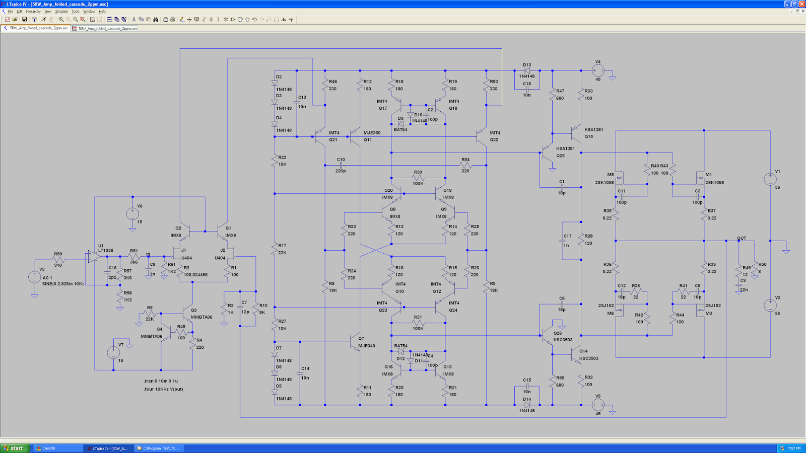
Just for you, +/-65V supplies, six pairs of output devices, and a follower (using LatFETs, because why not) on the VAS.
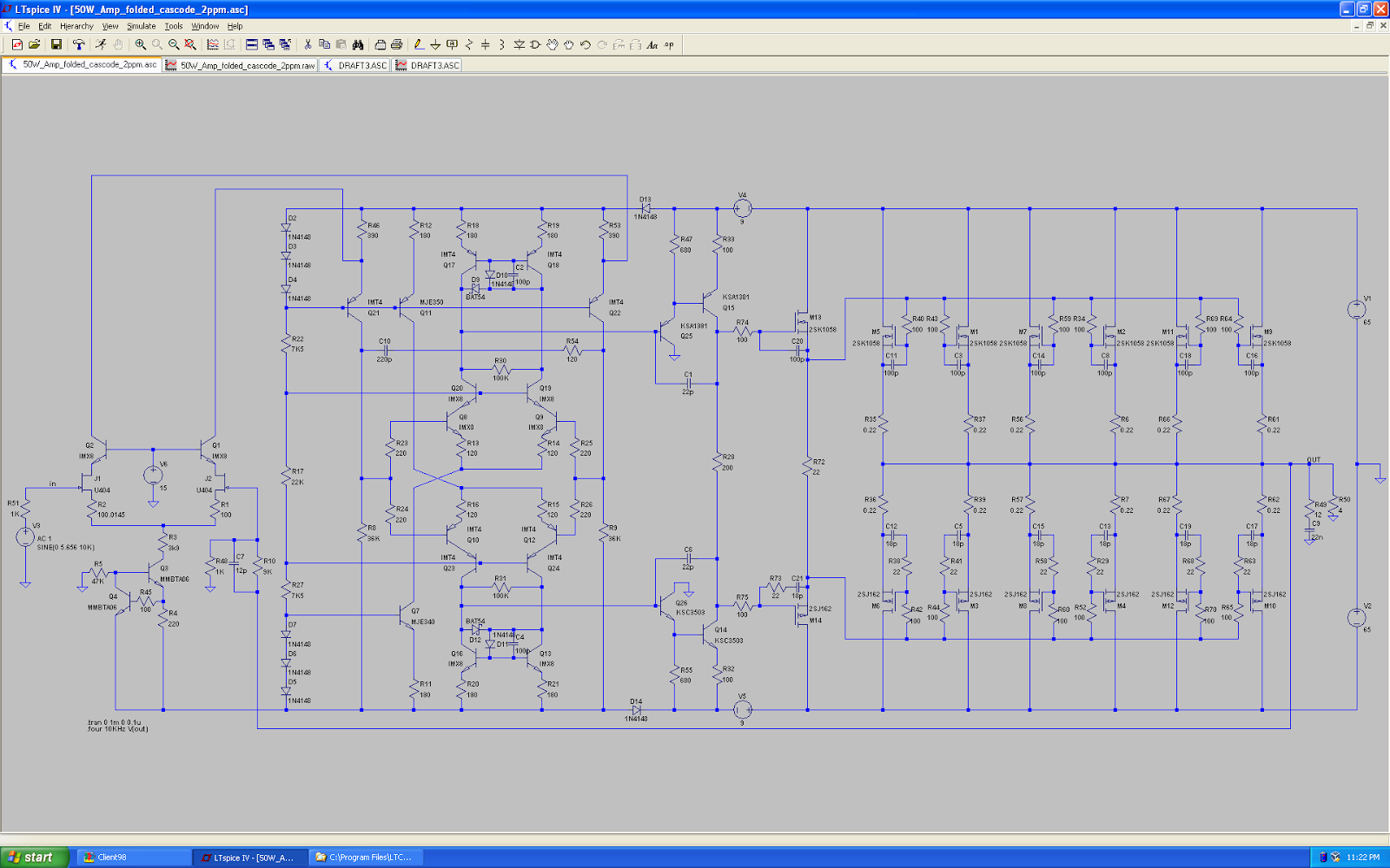
1 ppm THD, pushing 10KHz at 400W into 4 Ohms. I haven't done a SOA analysis for the output drivers - an extra couple of pairs would probably be prudent at these power levels.
You'll note that with the exception of a few resistor and capacitor value changes (I wound the bias down on the folded cascode to reduce dissipation and redid the compensation), everything up to the VAS is identical with the low power version.
Last edited:
I dunno, it appears you aren't brave enough to share the schematics for your amps
They are commercial amps; not smart to go public domain.
They are commercial amps; not smart to go public domain.
Indeed. And for commercial reasons it's also prudent to knock other's work without justification.
...1 ppm THD...
What models have you used for the OPS FETs?
I suspect they may be "optimistic" because your results don't look consistent with other, approximately comparable amps where the simulation has been validated.
I am curious to learn if there are simulation issues or why the circuit outperforms.
Best wishes
David
Every transistor in the circuit:
.MODEL 2SK1058 NMOS VTO=403.969M KP=20U L=2U W=29.7482M GAMMA=0 PHI=600M LAMBDA=184.988F RD=60.8251M CBD=2.56138N IS=10F CGSO=1.13517N CGDO=1.13517N TOX=0 NSUB=0 TPG=1 UO=600 RG=50 RDS=1MEG
.MODEL 2SJ162 PMOS VTO=842.193M KP=20U L=2U W=21.3317M GAMMA=0 PHI=600M LAMBDA=20.7067M RD=837.199M CBD=2.96862N IS=10F CGSO=1.13517N CGDO=1.13517N TOX=0 NSUB=0 TPG=1 UO=600 RG=50 RDS=1MEG
.MODEL U404 NJF(Beta=1.577m Betatce=-500m Rd=1 Rs=1 Lambda=10m Vto=-1.316 Vtotc=-2.5m Is=19.73f Isr=191.3f N=1 Nr=2 Xti=3 Alpha=68.56u Vk=212.2 Cgd=5.6p M=391.6m Pb=500m Fc=500m Cgs=6.044p Kf=4.592e-003f Af=1)
.MODEL MJE340 NPN(IS=1.03431e-13 BF=172.974 NF=0.939811 VAF=27.3487 IKF=0.0260146 ISE=4.48447e-11 NE=1.61605 BR=16.6725 NR=0.796984 VAR=6.11596 IKR=0.10004 ISC=9.99914e-14 NC=1.99995 RB=1.47761 IRB=0.2 RBM=1.47761 RE=0.0001 RC=1.42228 XTB=2.70726 XTI=1 EG=1.206 CJE=1e-11 VJE=0.75 MJE=0.33 TF=1e-09 XTF=1 VTF=10 ITF=0.01 CJC=1e-11 VJC=0.75 MJC=0.33 XCJC=0.9 FC=0.5 CJS=0 VJS=0.75 MJS=0.5 TR=1e-07 PTF=0 Vceo=300 Icrating=0.5A mfg=OnSemi)
.MODEL MJE350 PNP(IS=6.01619f BF=157.387 NF=0.910131 VAF=23.273 IKF=0.0564808 ISE=4.48479p NE=1.58557 BR=0.1 NR=1.03823 VAR=4.14543 IKR=0.0999978 ISC=1.00199e-13 NC=1.98851 RB=0.1 IRB=0.202965 RBM=0.1 RE=0.0710678 RC=0.355339 XTB=1.03638 XTI=3.8424 EG=1.206 CJE=1e-11 VJE=0.75 MJE=0.33 TF=1e-09 XTF=1 VTF=10 ITF=0.01 CJC=1e-11 VJC=0.75 MJC=0.33 XCJC=0.9 FC=0.5 CJS=0 VJS=0.75 MJS=0.5 TR=1e-07 PTF=0 Vceo=300 Icrating=0.5A mfg=OnSemi)
.MODEL IMX8 NPN (IS=14.6f NF=1.00 BF=581 VAF=197 IKF=30.4m ISE=2.54p NE=2.00 BR=4.00 NR=1.00 VAR=20.0 IKR=75.0m RE=0.830 RB=3.32 RC=0.332 XTB=1.5 CJE=12.5p VJE=1.10 MJE=0.500 CJC=4.02p VJC=0.300 MJC=0.300 TF=475p TR=80.1n EG=1.12 mfg=DiodesInc)
.MODEL IMT4 PNP (IS=60.000E-15 BF=410.23 VAF=58.369 IKF=.24851 ISE=60.000E-15 NE=1.6719 BR=.99563 VAR=100 IKR=.5153 ISC=26.592E-12 NC=1.6784 NK=.94666 RB=19.288 RC=2.0146 CJE=24.180E-12 MJE=.64498 CJC=11.927E-12 MJC=.47137 TF=381.07E-12 XTF=3.9957 VTF=6.2068 ITF=.11044 TR=790.19E-9 XTB=1.5000 mfg=Rohm)
.model MMBTA06 NPN (IS=50.8f NF=1.00 BF=479 VAF=161 IKF=91.1m ISE=9.99p NE=2.00 BR=4.00 NR=1.00 VAR=16.0 IKR=0.225 RE=0.103 RB=0.412 RC=41.2m XTB=1.5 CJE=58.7p VJE=1.10 MJE=0.500 CJC=18.9p VJC=0.300 MJC=0.300 TF=576p TR=110n EG=1.12 Vceo=80 Icrating=500m mfg=Fairchild)
.model MMBTA56 PNP (IS=50.8f NF=1.00 BF=479 VAF=161 IKF=91.1m ISE=9.99p NE=2.00 BR=4.00 NR=1.00 VAR=16.0 IKR=0.225 RE=0.103 RB=0.412 RC=41.2m XTB=1.5 CJE=125p VJE=1.10 MJE=0.500 CJC=40.2p VJC=0.300 MJC=0.300 TF=660p TR=149n EG=1.12 Vceo=80 Icrating=500m mfg=Fairchild)
.MODEL KSA1381 pnp IS=5.5544E-14 BF=148 BR=1.592 ISE=2.0546f NE=1.5 ISC=3.24807E-10 NC=2 VAF=580 VAR=100 IKF=0.2163 IKR=0.087544 RB=10.18 RE=0.0512 RC=4.072 CJE=9.572p VJE=0.748 MJE=0.371 FC=0.5 CJC=1.147p VJC=0.541 MJC=0.329 TF=1.0312E-09 XTB=0.907 EG=0.62 XTI=3
.MODEL KSC3503 NPN IS=2.0893E-14 BF=101.5 NF=1 BR=7.655 NR=1.007 ISE=4.3652E-14 NE=1.5 ISC=1.2598n NC=2 VAF=717.25 VAR=13.16 IKF=0.2512 IKR=0.0832 RB=2.98 RBM=0.001 IRB=0.001 RE=0.5305 RC=0.9 QCO=0.05 RCO=50.1187 VO=2.476 GAMMA=1.8231E-7 CJE=6.6039E-11 VJE=0.7017 MJE=0.3253 FC=0.5 CJC=6.6072p VJC=0.5 MJC=0.2439 XCJC=0.6488 XTB=1.4089 EG=1.2129 XTI=3 Vceo=300 Icrating=100m mfg=Fairchild
I don't remember how to attach an .asc file to a post. PM me an email address and I'll email it to you.
Last edited:
Would have to be present ubiquitously for intention you're implying, nope, couldn't be farther away from the truth. Simply my way to express admiration to your great work, using witty remark, apologizing if misunderstood. 🙂Indeed. And for commercial reasons it's also prudent to knock other's work without justification.
.MODEL 2SK1058 NMOS...
.MODEL 2SJ162 PMOS...
OK, that is what I suspected.
The NMOS and PMOS models are essentially for IC Mosfets and are seriously unrealistic for power Fets. They produce wonderfully optimistic results.
Bob Cordell's book covers the basics on better models but he has done a lot of extra work since LTspice made further improvements on the internal calculation model.
His latest work, on DIYaudio, is the most accurate that I know.
Best wishes
David
- Home
- Amplifiers
- Solid State
- Extending the AEM6000 design to ppm THD