I've built a number of amps over the years based on David Tilbrook's AEM6000. They've all been really good, reliable, low distortion, quiet amps. With the newer ones I've started departing a little from David's topology, initially by dispensing with one side of the VAS, which I built as a set of 50W modules that work very nicely, and now by realising that by dispensing with one side of the VAS, I can use current-mirror loads for the preceding stage, increasing the load impedance for that stage significantly and allowing for significantly better distortion performance.
I started discussing this in this thread http://www.diyaudio.com/forums/solid-state/288479-aem-6000-ready-build.html. Chalky pointed out that my VAS current wasn't well defined, being set from one side of a current mirror, so I've been working since then to get a handle on how to stabilise the VAS current without throwing away the gain. This initially involved using current sources and sinks tied back to the previous stage's tails, and more recently using a resistor across the mirror to define the collector voltage on the mirrored side at the cost of some gain.
While at it I changed out some of the VAS and preceding stage transistors, using the KSA1381/KSC3503 for the VAS, and IMX8/IMT4 duals for the preceding stages. Tail currents are provided by the cheap and cheerful MJE340/350.
I think I've reached a reasonable compromise with this, and I'm working now on layouts.
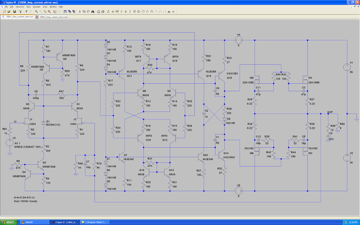
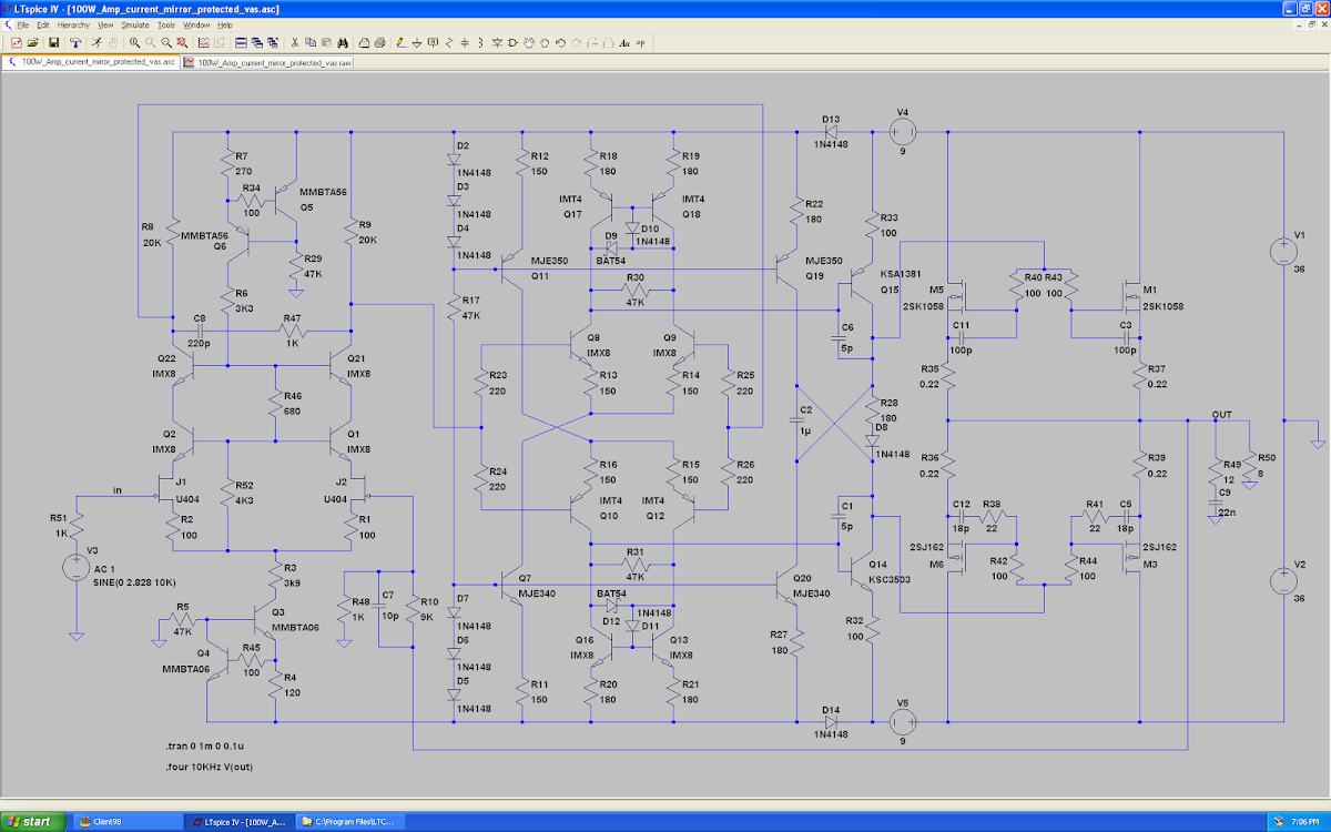
Here's the simulation schematic:
My goal with this is 1ppm THD at 1KHz/50W/8R, without huge supplies. I've set a somewhat arbitrary limit of 100mA bias for the LatFETs.
I've achieved this and then some. With gain set to 20dB, THD at 1KHz simulates at 0.4ppm, at 10KHz I achieve 3.5ppm, and even at 100KHz THD is a manageable 0.04%.
So, an explanation of how things work. The first stage is a completely conventional matched JFET (SST404), with cascode provided by an IMX8 dual and resistor loads. Tail current is set to 5mA, of which 3.5mA is used to bias the cascode and the rest flows through the JFETs.
The second stage is where I depart a little from David's topology. It's a symmetrical differential pair. Rather than the resistor loads of the AEM6000, I use a pair of current mirrors. Tail current for the differential pairs is set to a healthy 9mA. Dissipation is low enough that I can continue to use the IMX8/IMT4 duals both for the differential pairs and the current mirror loads, which is nice, as I really need a good match here, not to mention that these little things are lovely and fast, with plenty of gain at just the right current. I just use MJE340/350s for the tails as I don't need speed here but do need some dissipation.
Note R30 & R31. These 47K resistors waste some gain in this stage to ensure the collector voltages of Q17 & Q18 reasonably closely follow their mirrors. This allows us to define the VAS current by noting that the collector voltage here is defined by one Vbe + the current flowing through R18-22.
The current in the VAS is set by two mechanisms. The first is that for the VAS transistors (KSA1381/KSC3503 - Q14 & Q15). This is set by their emitter resistors. They have constant current loads (Q19 & Q20), whose currents are set by their emitter resistors, recycling the reference from the preceding stage tails.
The loads must be set at a lower current than the VAS transistors, to ensure current flows through R28, and hence the bias for the final stage drivers is set. I chucked a diode in here (thanks PB2), because if the VAS transistors and loads aren't biased correctly there was otherwise nothing to stop current from flowing the wrong way through R28.
I run the VAS transistors at 10mA, and the loads at a tad over 7mA, leaving the balance of a little over 2mA flowing through R28. This is then tweaked to give me 100mA driver bias.
Compensation is straightforward. A couple of caps across the VAS transistors, some RC across the first stage diffamp, and normal phase-lead compensation at the feedback point. I can push the gain all the way down to 3 (1ppm at 10KHz!) without it taking off, so I'm confident that it can be reasonably easily stabilised at more usual voltage gain levels.
Anyway, I think it's cool. I'm gonna build a couple, and I'd appreciate critique, especially of my logic around the VAS current stabilisation mechanism, as this is the area where I'm least confident.
I started discussing this in this thread http://www.diyaudio.com/forums/solid-state/288479-aem-6000-ready-build.html. Chalky pointed out that my VAS current wasn't well defined, being set from one side of a current mirror, so I've been working since then to get a handle on how to stabilise the VAS current without throwing away the gain. This initially involved using current sources and sinks tied back to the previous stage's tails, and more recently using a resistor across the mirror to define the collector voltage on the mirrored side at the cost of some gain.
While at it I changed out some of the VAS and preceding stage transistors, using the KSA1381/KSC3503 for the VAS, and IMX8/IMT4 duals for the preceding stages. Tail currents are provided by the cheap and cheerful MJE340/350.
I think I've reached a reasonable compromise with this, and I'm working now on layouts.
Here's the simulation schematic:
My goal with this is 1ppm THD at 1KHz/50W/8R, without huge supplies. I've set a somewhat arbitrary limit of 100mA bias for the LatFETs.
I've achieved this and then some. With gain set to 20dB, THD at 1KHz simulates at 0.4ppm, at 10KHz I achieve 3.5ppm, and even at 100KHz THD is a manageable 0.04%.
So, an explanation of how things work. The first stage is a completely conventional matched JFET (SST404), with cascode provided by an IMX8 dual and resistor loads. Tail current is set to 5mA, of which 3.5mA is used to bias the cascode and the rest flows through the JFETs.
The second stage is where I depart a little from David's topology. It's a symmetrical differential pair. Rather than the resistor loads of the AEM6000, I use a pair of current mirrors. Tail current for the differential pairs is set to a healthy 9mA. Dissipation is low enough that I can continue to use the IMX8/IMT4 duals both for the differential pairs and the current mirror loads, which is nice, as I really need a good match here, not to mention that these little things are lovely and fast, with plenty of gain at just the right current. I just use MJE340/350s for the tails as I don't need speed here but do need some dissipation.
Note R30 & R31. These 47K resistors waste some gain in this stage to ensure the collector voltages of Q17 & Q18 reasonably closely follow their mirrors. This allows us to define the VAS current by noting that the collector voltage here is defined by one Vbe + the current flowing through R18-22.
The current in the VAS is set by two mechanisms. The first is that for the VAS transistors (KSA1381/KSC3503 - Q14 & Q15). This is set by their emitter resistors. They have constant current loads (Q19 & Q20), whose currents are set by their emitter resistors, recycling the reference from the preceding stage tails.
The loads must be set at a lower current than the VAS transistors, to ensure current flows through R28, and hence the bias for the final stage drivers is set. I chucked a diode in here (thanks PB2), because if the VAS transistors and loads aren't biased correctly there was otherwise nothing to stop current from flowing the wrong way through R28.
I run the VAS transistors at 10mA, and the loads at a tad over 7mA, leaving the balance of a little over 2mA flowing through R28. This is then tweaked to give me 100mA driver bias.
Compensation is straightforward. A couple of caps across the VAS transistors, some RC across the first stage diffamp, and normal phase-lead compensation at the feedback point. I can push the gain all the way down to 3 (1ppm at 10KHz!) without it taking off, so I'm confident that it can be reasonably easily stabilised at more usual voltage gain levels.
Anyway, I think it's cool. I'm gonna build a couple, and I'd appreciate critique, especially of my logic around the VAS current stabilisation mechanism, as this is the area where I'm least confident.
Last edited:
Suzyj
I follow your work since I showed it in old littlefisch site.
You made a great work and a impressive and nice layout. Congratulations
I also need to introduce my self after give you some suggestion, I am an old test engineer that worked for long time in a big name Telecom company.
Personally I do not like smd device as it is a bit hard to find in Brazilian parts market and to help i have some difficulties to make assemblies with it(slow hands and weak eyes).
I kindly ask you to consider using LED as voltage reference instead of 1N4148 diodes string as it can decrease the parts count and they can make a very good voltage reference. I think it is a good practice to use a capacitor in parallel with then to improve a bit PSRR unless you plan to use a stabilized voltage regulator to signal amplifier.
I also can ask you to share your asc file and models as I can draw some proposal to you think about.
Kindest Regards and very happy new year
Ronaldo
hi suzyj,
thanks for sharing.
on a quick look, the vas logic makes sense to me. i'll think about it some more and comment if i change my mind.
however, one question i have is how will this stage behave when clipping?
btw, i'll mention again adding base resistors for current source/sink feedback transistors (Q4, Q5) is free insurance against oscillation risk/worries in those areas.
good work!
mlloyd1
Hi mlloyd,
Ahah! Thanks for the suggestion of checking clipping.
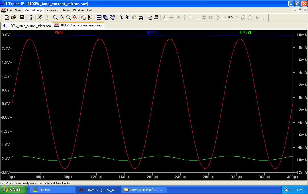
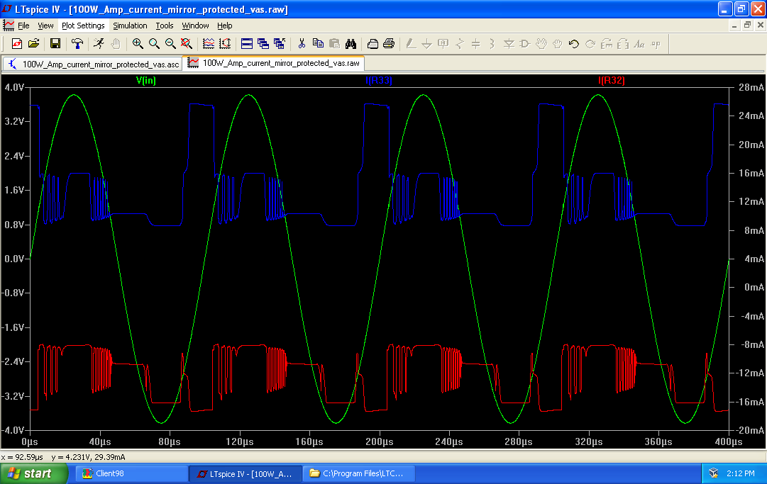
Here's normal response. Red is input, blue and green are VAS currents. Everything's happy.
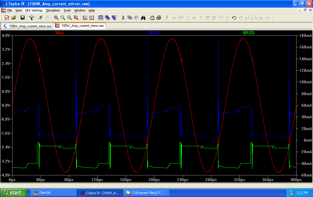
However once we push the amp into clipping the VAS current goes nuts. This would undoubtedly result in destruction of the VAS transistors:
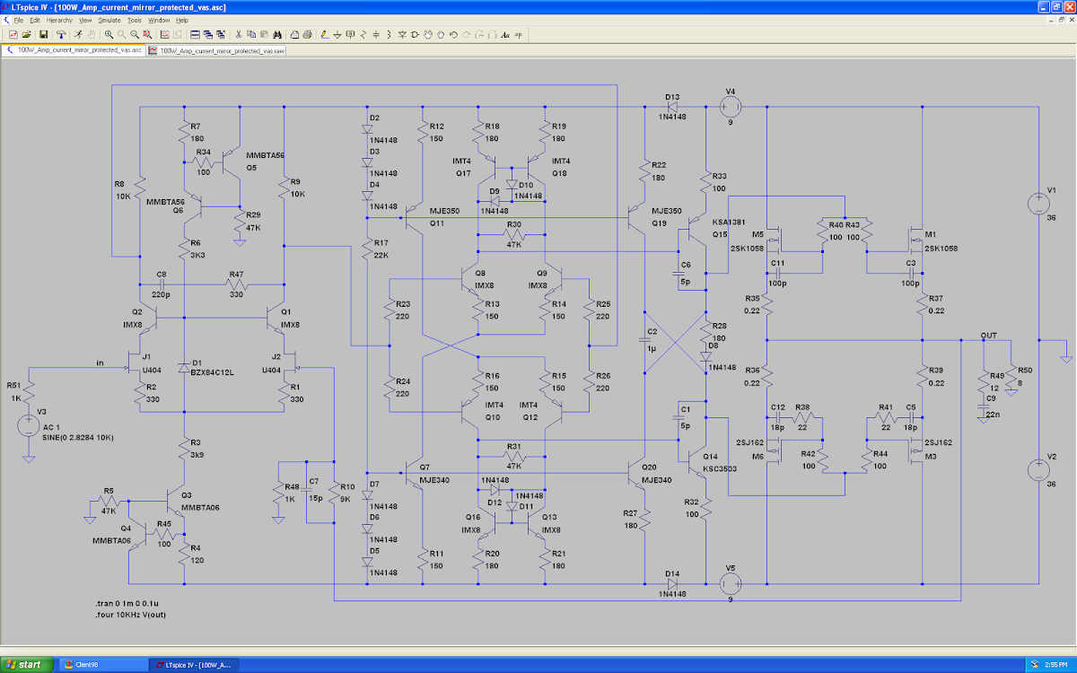
I spent some time trying to come up with a way to hard-limit the VAS current without introducing distortion. The following at least ensures the VAS will survive clipping, limiting current to ~2.5 times normal. It's based on some of the circuitry from Stochino's amp (the two diodes in the mirror), plus a couple of extra diodes in series with the supply rails to allow me to more accurately set VAS current. Oh, and I added base resistance to the input stage current sources as well, thanks for that tip:
10KHz THD is now 4ppm, so still not too bad. VAS current is ugly on clipping (note the oscillation) but at least is held within reasonable limits. I think it's likely to damage tweeters if this behaviour is allowed - an output choke (or better yet an op-amp hard limiter on the input) would probably be mandatory for hard use.
Ahah! Thanks for the suggestion of checking clipping.
Here's normal response. Red is input, blue and green are VAS currents. Everything's happy.
However once we push the amp into clipping the VAS current goes nuts. This would undoubtedly result in destruction of the VAS transistors:
I spent some time trying to come up with a way to hard-limit the VAS current without introducing distortion. The following at least ensures the VAS will survive clipping, limiting current to ~2.5 times normal. It's based on some of the circuitry from Stochino's amp (the two diodes in the mirror), plus a couple of extra diodes in series with the supply rails to allow me to more accurately set VAS current. Oh, and I added base resistance to the input stage current sources as well, thanks for that tip:
10KHz THD is now 4ppm, so still not too bad. VAS current is ugly on clipping (note the oscillation) but at least is held within reasonable limits. I think it's likely to damage tweeters if this behaviour is allowed - an output choke (or better yet an op-amp hard limiter on the input) would probably be mandatory for hard use.
Last edited:
Welcome back to the insanity that is DIY Audio, suzyj ")
I guess the purpose of V4 and V5 in the schematic is to represent a slightly higher voltage for the input LTP and voltage gain stages? If so, you may find that a signal diode from the base of your driver transistors (Q14 and Q15) to the output devices power rails (V1 and V2) works well to tame any VAS stage sticking going on.
Also, as I have found on my own design, these higher voltages can be readily generated by a Greinacher/Cockroft type multiplier followed by a Zener regulator. For the small amounts of current drawn by these stages, it works very well and saves having to custom wind a transformer
R7 allows ~3.5mA to pass through D1.Tail current is set to 5mA, of which 3.5mA is used to bias the cascode and the rest flows through the JFETs.
R4 allows ~5mA to pass through R3.
That means the LTP is under 1mA per side.
Did you intend to operate at this low current?
R1 & R2 are quite high for a jFET LTP. Noise?
No RF filter?
No DC protection?
Last edited:
Closed loop gain is set to 10, or 20dB. My intention is to have an opamp stage before this, with around 10dB gain, so noise performance isn't terribly important. That said, ~1mA per side gives me a reasonable 5 odd nv/sqrtHz measured on my existing amps, and the SST404 is a pretty low current part, with saturation current specified as 3.5mA min. I haven't bothered to simulate the input filters as they're not that interesting.
Still, this is an area of the design I haven't really played with in years. It might be a spot where improvements are easy to find.
Still, this is an area of the design I haven't really played with in years. It might be a spot where improvements are easy to find.
Last edited:
set your gain to +30dB (1:30 gives you 31times) and you don't need the extra stage.Closed loop gain is set to 10, or 20dB. My intention is to have an opamp stage before this, with around 10dB gain,..............
Last edited:
Hi Suzy, Did you consider the standard VAS clamp that senses the emitter current and clamps the drive? In this situation the previous stage is a diff amp so it is limited by the tail current. Also, diodes across the front end diff pair should help and are a very simple solution, might even be enough.
I know you can figure this out but for others, Bob C. covers them in his Hafler mod slides:
http://www.diyaudio.com/forums/atta...lifier-book-cordell_burningamp2016_dh220c.pdf
I know you can figure this out but for others, Bob C. covers them in his Hafler mod slides:
http://www.diyaudio.com/forums/atta...lifier-book-cordell_burningamp2016_dh220c.pdf
Last edited:
What I have by now with very different results.
I am following the circuits here with the exception of gain transistor.
Share the gain is a option to the person doing the project. I would like to listen the reason.
I am following the circuits here with the exception of gain transistor.
Share the gain is a option to the person doing the project. I would like to listen the reason.
Attachments
What is the reason to share gain between 2 stages?
Of course increasing the gain you will have more distortion, but you can manage this in project of the amplifier itself.
Could you please send me models for IMX8 and IMT4.
Thanks
Keeping the closed loop gain down helps to reduce distortion. It also allows me to take the benefit of a low noise input opamp to reduce the noise even further.
Here's my models for the IMX8 & IMT4. You won't like them at all, as they're a six legged SOT-23
Code:
.MODEL IMX8  NPN (IS=14.6f NF=1.00 BF=581 VAF=197 IKF=30.4m ISE=2.54p NE=2.00 BR=4.00 NR=1.00 VAR=20.0 IKR=75.0m RE=0.830 RB=3.32 RC=0.332 XTB=1.5 CJE=12.5p VJE=1.10 MJE=0.500 CJC=4.02p VJC=0.300 MJC=0.300 TF=475p TR=80.1n EG=1.12 mfg=DiodesInc)

.MODEL IMT4  PNP (IS=60.000E-15 BF=410.23 VAF=58.369 IKF=.24851 ISE=60.000E-15 NE=1.6719 BR=.99563 VAR=100 IKR=.5153 ISC=26.592E-12 NC=1.6784 NK=.94666 RB=19.288 RC=2.0146 CJE=24.180E-12 MJE=.64498 CJC=11.927E-12 MJC=.47137 TF=381.07E-12 XTF=3.9957 VTF=6.2068 ITF=.11044 TR=790.19E-9 XTB=1.5000 mfg=Rohm)
Last edited:
What I have by now with very different results.
I am following the circuits here with the exception of gain transistor.
Share the gain is a option to the person doing the project. I would like to listen the reason.
Why the 60V supplies? 36V is oodles for 50W into 8 Ohms (28Vpeak).
Hi Suzy, Did you consider the standard VAS clamp that senses the emitter current and clamps the drive? In this situation the previous stage is a diff amp so it is limited by the tail current. Also, diodes across the front end diff pair should help and are a very simple solution, might even be enough.
I know you can figure this out but for others, Bob C. covers them in his Hafler mod slides:
http://www.diyaudio.com/forums/atta...lifier-book-cordell_burningamp2016_dh220c.pdf
I hadn't seen that before, so thankyou very much for sharing it. Cordell is a terribly smart cookie. I can see the next few days evaporating in a design frenzy based on his cool mirror clamp ideas.
Here's my reason for the 36V supplies, by the way:
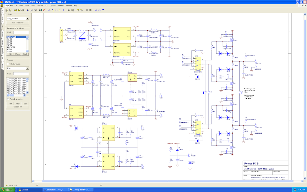
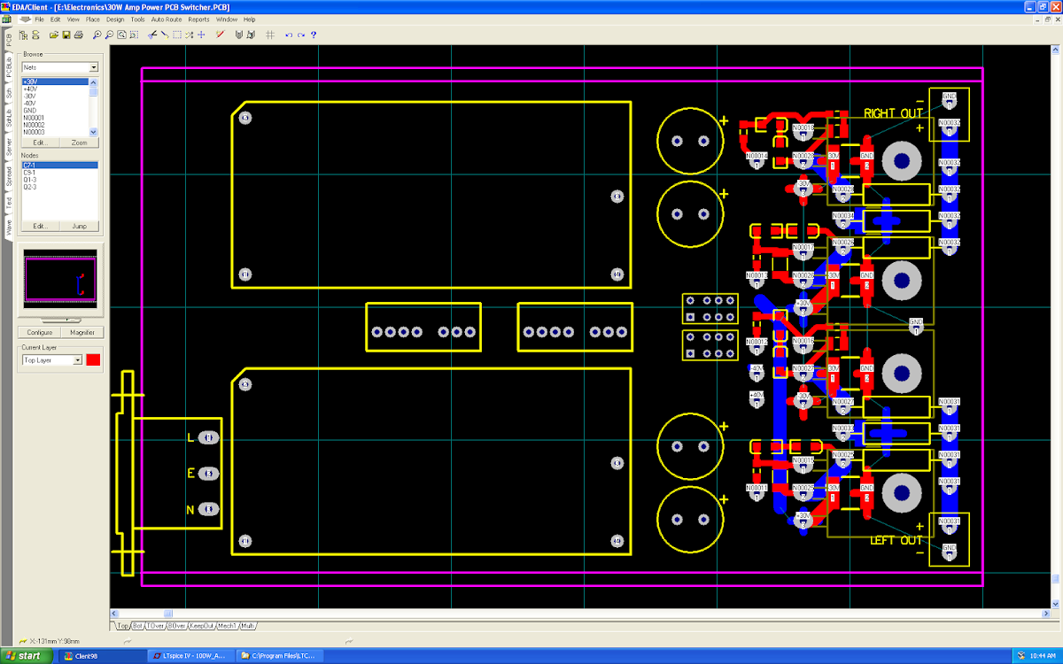
I can buy very nice little 36V, 30W PCB mount switchers from XP power (EML30) that are just 75 x 35 footprint. Two of these fit quite nicely along with all the other high-power parts on a 160 x 100 PCB:
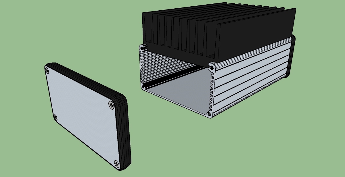
Which then fits nicely in a Hammond 1455 enclosure, making use of a slightly modified Fisher 43DN 100 x 150 x 40 heatsink:
I can buy very nice little 36V, 30W PCB mount switchers from XP power (EML30) that are just 75 x 35 footprint. Two of these fit quite nicely along with all the other high-power parts on a 160 x 100 PCB:
Which then fits nicely in a Hammond 1455 enclosure, making use of a slightly modified Fisher 43DN 100 x 150 x 40 heatsink:
While playing with input diffamp current doesn't do terribly much, adding a second cascode to the input diffamp is quite useful. 10KHz THD into 50W, 8R is now under 2ppm:
BAT54 schottky rectifiers do a better job of controlling the VAS current than the LL4148 silicon rectifiers do(max VAS current ~21mA rather than 25), and their added capacitance (10p vs ~1p) doesn't appear to mess stability up. I might try a BAS40 instead (~2.5p) but I'll have to find a model for that.
Bumping the supplies up to +/-48V allows 10KHz 2ppm THD driving 100W into 8R with no circuit changes at all.
And this is where the cascode rabbit hole leads.
I started by folding the second cascode on the input diffamp. My reasoning for this was twofold. Firstly I wanted to get the C-E voltages better balanced in the symmetrical second stage, and additionally I wanted to try cascoding the second stage, and needed more headroom in the top half to do that. I biased the folded cascode from the existing diode string for the second stage, so there aren't any additional parts.
Next I removed the current loads for the VAS. They weren't really doing anything useful now that I'd better controlled the VAS current by clamping the preceeding diffamps. I substituted grounded collector transistors on the VAS bases. These work quite well in this application, as the additional Vbe drop means the VAS current is much better controlled than with the single transistor.
I added some capacitance in the current mirror to provide better HF stability.
I added cascodes to the second stage diffamps. I used IMX8 and IMT4 duals. This didn't really add any appreciable performance, as the IMX8 are already plenty fast, but it does allow me to keep dissipation in the transistors down to about 150mW despite running them at 5mA.
Here's the schematic:
As per my self imposed arbitrary rule, I'm running off +/-36V supplies for the FETs, with +/-45V for everything else. Current draw from my +/-45mA supply is 45mA, or 4W. I'm burning 15W quiescent in the LatFETs (100mA per device), so it won't burn the house down.
10KHz, 50W 8R THD is now 1.0ppm (0.000100%). 1KHz, 50W 8R THD is 0.07ppm (0.000007%). And with +/-48V main supplies, I get 1.08ppm (10KHz, 100W), and 0.07ppm (1KHz, 100W). I really can't see any point in pushing this any further. Indeed I think I'll be backing off a tad from here.
Last edited:
I've tried grafting an additional stage in previously, but gotten absolutely nowhere. I couldn't stop it oscillating whatever I did. The cascodes, to the contrary, have been really quite straightforward, albeit providing incremental improvements only. The folded cascode was very worthwhile though, as it allows increasing the gain of the input diffamp significantly.
The challenge here was getting the VAS current stable with the current mirror load. That proved to be quite a fun intellectual exercise.
One thing I really like about this topology, and the AEM6000 in general, is the degree of PSRR. I measure 95dB in simulation. It means I can be really unfussy about power supply ripple. As long as it's under a hundred millivolts or so I'll never hear it.
The current transfer ratio of a simple current mirror is only about 0.8 something so I guess different collector voltages are to be expected. The 47k resistors help in this respect but why didn't you opt for helper transistors like Cordell uses? Might be even better if you used one of the 4 transistor current mirrors. You'd get an almost unity current transfer ratio and pretty closely matched collector voltages. You might then be able to dispense with the 47k resistors and the attendant loss of olg?
- Home
- Amplifiers
- Solid State
- Extending the AEM6000 design to ppm THD