Thanks for sharing. Can you do the same for NPN BJT ?
http://www.diyaudio.com/forums/soli...al-npn-no-quasi-saturation-measured-data.html
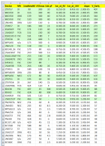
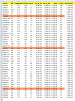
I added several more PNPs to the table today, new entries are marked in green. Sanyo lovers: your favorite is found in row #17.
When there was no "Cob" listed in the tabulated information in the datasheet, but there was a "Cob" graph, I chose the lowest-voltage datapoint (with the highest Cob) to enter into my table. Perhaps this is more pessimistic than the measurement point used by other transistors. But if they don't even spec it, should I even try to tabulate it? Hmm.
When there was no "Cob" listed in the tabulated information in the datasheet, but there was a "Cob" graph, I chose the lowest-voltage datapoint (with the highest Cob) to enter into my table. Perhaps this is more pessimistic than the measurement point used by other transistors. But if they don't even spec it, should I even try to tabulate it? Hmm.
Attachments
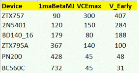
Beta and Early are inversely related (as I'm sure you observed).
Not an exact proportion for all devices. ZTX795A seems to be a happy design.
Beta and VCEmax "should" be related as square-root of Beta, for some idealized geometry (AS Grove). The root relation is not clear in your data. Possibly real geometries, possibly geometry and specs tweaked for different intended markets.
Attachments
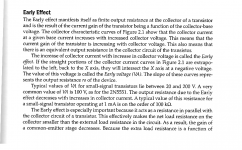
Wikipedia has an article that discusses the Early voltage.
Bob Cordell's book also covers it. I've copied the very first mention (on page number 19 of a 600 page book!) below.
_
Bob Cordell's book also covers it. I've copied the very first mention (on page number 19 of a 600 page book!) below.
_
Attachments
Robert Pease wrote an article on transistor Mu vs Beta and pointed out that they are inversely related. Higher Beta means lower Mu. Mu can be approximated by dividing the Early voltage by the thermal voltage. Of course Mu is also 1/Hre so you can estimate the Early voltage from that transistor parameter.
The Pease article is available at: What's All This VBE Stuff, Anyhow? (Part 2) | Power content from Electronic Design
You have mis-remembered the part in red above. Consulting Pease's article he said "mu = 1/hRB"
Added three more rows (transistor types).
Added a new column: Beta x Vearly figure of merit, and sorted the data by this F.O.M.
Found additional sources of information that let me update several "Cob" entries.
The Sanyo device that Bob Cordell's book is so enthusiastic about, finishes 31st best out of 44 transistors according to this F.O.M. Which in a way is probably a good thing; this little exercise has identified 30 transistors that are even better than the 2SA1407E.
_
Attachments
Electrician,
I emailed Robert Pease some questions about the article and he informed me that Hre and Hrb are for all practical purposes identical. To verify that Mu equals 1/Hre just convert H parameters to abcd (transfer) parameters. The abcd parameters relate the output voltage and current to the input voltage and current and are as follows.
Voltage gain Mu=Vo/Vi
Current gain Alpha=Io/Ii
Transadmitance =Io/Ei
Transresistance=Eo/Ii
If you look at the conversion table for converting H to abcd parameters, you see that Mu=1/Hre.
Pease says that (beta * mu) is one million, as a rule of thumb (attached).
So for the BC327-40 transistor, whose measured beta is 430 (and whose datasheet guarantees 250 < beta < 630), mu is 2325.
I can't for the life of me find anything on a BC327-40 whose value is 2325. Its output conductance (hybrid pi parameter "ro") at Vce=5V and Ice=1ma, is 49 kilohms. Its maximum CE voltage gain (namely, gm * ro) is 1880 volts per volt. Maybe Pease is saying that 1880 is about the same as 2325 (?)
If so then
For really excellent transistors, Vearly is enormously larger than Vce so we can neglect the Vce term, simplifying the expression a bit. Now it includes beta*Vearly (the Figure Of Merit!) and some multiplicative constants.
_
So for the BC327-40 transistor, whose measured beta is 430 (and whose datasheet guarantees 250 < beta < 630), mu is 2325.
I can't for the life of me find anything on a BC327-40 whose value is 2325. Its output conductance (hybrid pi parameter "ro") at Vce=5V and Ice=1ma, is 49 kilohms. Its maximum CE voltage gain (namely, gm * ro) is 1880 volts per volt. Maybe Pease is saying that 1880 is about the same as 2325 (?)
If so then
- mu ?=? gm * ro
- mu ?=? (Ice / 26mV) * (Vce + Vearly)/Ice
- mu ?=? (Vce + Vearly) / 26mV
- 1 million ?=? beta * mu
- 1 million ?=? beta * (Vce + Vearly) / 26mV
For really excellent transistors, Vearly is enormously larger than Vce so we can neglect the Vce term, simplifying the expression a bit. Now it includes beta*Vearly (the Figure Of Merit!) and some multiplicative constants.
_
Attachments
Electrician,
I emailed Robert Pease some questions about the article and he informed me that Hre and Hrb are for all practical purposes identical. To verify that Mu equals 1/Hre just convert H parameters to abcd (transfer) parameters. The abcd parameters relate the output voltage and current to the input voltage and current and are as follows.
Voltage gain Mu=Vo/Vi
Current gain Alpha=Io/Ii
Transadmitance =Io/Ei
Transresistance=Eo/Ii
If you look at the conversion table for converting H to abcd parameters, you see that Mu=1/Hre.
Could you post the conversion table, or a link to one?
If I use the one here: https://en.wikipedia.org/wiki/Two-port_network
down near the bottom under the heading "Interrelation of parameters", I don't get Pease's result.
Edit: OK. I see that 1/hre is not the exact expression, but it's a very good approximation depending on the product hie*hoe being very small.
Last edited:
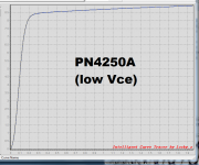
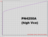
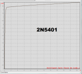
After staring at the data for a while, I chose a cascode combination: PN4250A for the "inner" device (the one whose VCE is fixed and constant thanks to cascoding), and 2N5401 for the "cascode" device (the one whose collector sees all the signal swing).I'm building current sources and current mirrors that run at about 8mA of bias, and trying to decide which device types to select.
Since I don't want the current source to gobble up tons of supply headroom, I'm operating the inner device at relatively low VCE: 1.25 volts. I decided that means I want an inner device whose "knee" is well to the left of (1.25V @ 8mA). The PN4250A seems to do this quite effortlessly, while having a relatively high Beta (300) and low Cob (6pF).
I wanted a cascode device with high Early voltage, decent Beta, low Cob, and good IV behavior at low VCE. The 2N5401 seems to fit the bill.
LTSPICE simulation says this cascode current source has an output impedance of about 6 megohms at midband, which is more than good enough because the input impedance of subsequent circuitry is a lot lower.
Now to lay it out!
Attachments
Typically Hoe*Hie is much less than 1.0. A small signal transistor running a few mA collector current might have an input resistance of 2k and an output resistance of 100k. Hoe*Hie is then 2/100 or .02 which is much less than 1.0 and can usually be ignored.
In the case of the common emitter h parameters, it's not so much whether hoe*hie is less than one; it's whether hoe*hie is much less than hfe*hre.
I went looking for some typical h parameters on the web and the first thing I found was this: https://www.scribd.com/doc/19521971/h-Parameters-Conversion
The values given there are:
hie = 1200
hre = .0002
hfe = 100
hoe = .00002
Using these values and converting to ABCD parameters, I get a value for mu of -25000, which I take to be the correct value.
The value of 1/hre is 5000
Converting the common emitter parameters to common base parameters, I get -1/hrb = -26580. This is a better approximation than 1/hre.
For the given h parameters, hie*hoe = .024 and hfe*hre = .02
These values are nearly the same, and that being so, the approximation for mu of 1/hre is greatly different from the value (the truly correct value) given by conversion to ABCD parameters.
Have you tried the various formulas and approximations with some typical values for transistor common emitter h parameters? What results do you get?
I just use the conversion formulas in my reference book which is the same as the formulas in the wiki article on two port networks. Where did you get your conversion formulas?
I use the ones here: https://en.wikipedia.org/wiki/Two-port_network
down near the bottom under the heading "Interrelation of parameters"
What kind of results do you get if you try out some typical groups of transistor common emitter h parameters?
I am confused.
In the wiki the conversion formulas for what they call "b" parameters are,
b11=1/H12
b12=-H11/H12
b21=-H22/H12
and b22=delta[H]/H12.
These are the same formulas in my reference book except they call the b parameters abcd parameters which is the name I used.
How did you get mu=((hrb-1)*hfb-hib*hob)/(hrb*hfb-hib*hob) ?
I am confused.
In the wiki the conversion formulas for what they call "b" parameters are,
b11=1/H12
b12=-H11/H12
b21=-H22/H12
and b22=delta[H]/H12.
These are the same formulas in my reference book except they call the b parameters abcd parameters which is the name I used.
How did you get mu=((hrb-1)*hfb-hib*hob)/(hrb*hfb-hib*hob) ?
On the Wikipedia page: https://en.wikipedia.org/wiki/Two-port_network
about half way down, under the heading "ABCD-parameters", is some discussion of the difference between ABCD parameters and A'B'C'D' parameters. A'B'C'D' parameters are the same as "b" parameters, and ABCD parameters are the same as "a" parameters. To be clear, the elements of the matrices are:
A = a11
B = a12
C = a21
D = a22
and
A' = b11
B' = b12
C' = b21
D' = b22
The relationship between the "a" parameters and the "b" parameters is that the "b" parameter matrix:
[ b11 b12 ]
[ b21 b22 ]
is the inverse of the "a" parameter matrix:
[ a11 a12 ]
[ a21 a22 ]
equivalently A'B'C'D' = Inverse[ABCD]
The significance of a11 is different from b11.
1/a11 is the forward voltage gain of the two-port represented by the "a" matrix, but 1/b11 is not the same. 1/b11 is the reverse voltage gain of the two-port.
You said your reference book calls "b" parameters abcd parameters. Does this reference distinguish between abcd parameters and ABCD parameters? Does it talk about "a" parameters at all, or only about "b" parameters.
- Home
- Amplifiers
- Solid State
- Measuring the Early voltage "VA" of some PNPs at 8mA