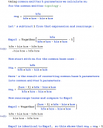
How did you get mu=((hrb-1)*hfb-hib*hob)/(hrb*hfb-hib*hob) ?
Since mu is the voltage gain of a common emitter stage, when you're deriving mu from the common base h parameters, it's necessary to convert those CB h parameters to common emitter h parameters first, then convert to ABCD parameters. Doing all this should get the expression you're asking about.
Now I understand. If you look at the exact formulas for the voltage gains of CB and CE amplifying stages, they are practically identical. The approximate formulas are identical and this means the mu's of the CB and CE amplifiers are practically identical and thus Hrb and Hre are practically identical. That is what Bob Pease stated. You really don't need to perform all those calculations. Note. I am using the book, Reference Data For Radio Engineers by ITT.
Last edited:
Common emitter gain = Zcollector / (Zemitter + (1/gm))
If the collector load is an ideal current source then Zcollector is only the common emitter amplifying transistor's ro.
If there is no emitter resistor then the expression simplifies to: CEgain = gm*ro
If the transistor's operating point is (VCE, ICE) then ro = (Vearly + VCE)/ICE
And CEgain = gm * (Vearly + VCE) / ICE
Since gm = ICE/Vthermal {where Vthermal = kT/q = 26 mV at room temperature}
CEgain = (Vearly + VCE) / Vthermal
For good transistors with Vearly >>> VCE
CEgain = Vearly / Vthermal
Responding to the question about the difference between the ABCD (cascade) parameters and the abcd (transfer) parameters. I know the difference. The ABCD (capital letters) parameters relate the input voltage and current to the output voltage and current and the abcd (small letters) parameters relate the output voltage and current to the input voltage and current. I am very familiar with the two port parameters. In the 1970s I wrote a Fortran computer program to convert the two port parameters from one parameter set to another. At first this looked like a formidable programming effort because there are six different two port parameters so five conversions were needed for each parameter. That's thirty conversions and each parameter set has 4 quantities so at first that looks like 120 conversion formulas. However when you look at the conversion formulas you see that many of them have the same form so only about 20 different conversion formulas are actually required. It's a whole lot easier to program 20 conversion formulas instead of 120 conversion formulas.
Now I understand. If you look at the exact formulas for the voltage gains of CB and CE amplifying stages, they are practically identical. The approximate formulas are identical and this means the mu's of the CB and CE amplifiers are practically identical and thus Hrb and Hre are practically identical. That is what Bob Pease stated. You really don't need to perform all those calculations. Note. I am using the book, Reference Data For Radio Engineers by ITT.
Can you come up with some numerical common base h parameters so we can test how well 1/hrb = mu?
I can only find numerical common emitter h parameters, so conversion to common base is needed. I'm away from my library, but later today I should be able to find a table of conversion among common base, common collector and common emitter h parameters.
Now I understand. If you look at the exact formulas for the voltage gains of CB and CE amplifying stages, they are practically identical.
This is true and it can be shown that the gain for the CB stage is equal to the gain for the CE stage minus 1 (possible neglecting signs). Since gains are usually >>1, this verifies that they are "pratically identical":
The approximate formulas are identical and this means the mu's of the CB and CE amplifiers are practically identical and thus Hrb and Hre are practically identical. That is what Bob Pease stated. You really don't need to perform all those calculations. Note. I am using the book, Reference Data For Radio Engineers by ITT.
The part in red doesn't necessarily follow. Testing it with typical numerical data for CB and CE h parameters would be informative.
The numerical CE h parameters I referenced in post #36 don't support the supposition that mu for the CE case is nearly the same as 1/hre.
I think this can be seen from the exact expression for mu for the CE case:
hfe/(hfe*hre-hie*hoe)
This can only equal (or be close to) 1/hre if the value of hie*hoe is negligible compared to hfe*hre. For the parameters in post #36 it's not true.
Can you find some numerical values for h parameters and compare the exact mu with 1/hre?
Attachments
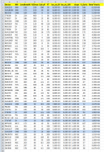
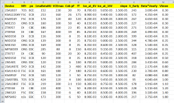
I added measurement data from a few more PNP transistors; mostly they are devices I learned about when reading this diyAudio thread. The new devices are shaded in blue.
_
_
Attachments
I calculated Bob Pease's "Rule Of Thumb" from his Electronic Design magazne article linked in post #27 above.
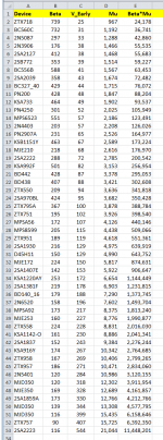
His rule is that (Beta times Mu) is about two million; in some cases one, other cases four. I tabulated that number below. Remember, these are PNP discrete transistors. Click on the funny "X" in the lower left corner of the image, to magnify it up to full size for good readability.
_
His rule is that (Beta times Mu) is about two million; in some cases one, other cases four. I tabulated that number below. Remember, these are PNP discrete transistors. Click on the funny "X" in the lower left corner of the image, to magnify it up to full size for good readability.
_
Attachments
Last edited:
Thanks for all the information here. Would someone please post a link to a thread or article that shows how the Early Voltage of a transistor affects a circuit in context of it intended design. I never have been comfortable with its named after its creator, it unintentionally implies something that it is not. Like a Banker being named Mr. Crook. Maybe that is not a good analogy after all. A LTSpice diagram would be a BIG plus.
Thanks in advance to all the Transistor Gurus this site is blessed with.
Thanks in advance to all the Transistor Gurus this site is blessed with.
> how the Early Voltage of a transistor affects
Do you know vacuum tubes?
"Plate resistance". Rp
Given an ideal infinite load (never happens), maximum voltage gain is Rp*Gm.
Gm is affected by current. We have a very rough idea on a tube. BJT Gm is (if no stray resistance) known exactly from Shockley's Law.
Rp is a measure of how plate voltage "leaks back" to the input circuit.
Pentode Rp may be very high.
Pentode plate curves are typically curved. High Rp at high voltage but falling off at low voltage.
BJT "plate curves" are a lot straighter (when well below Vceo Max).
The funny thing is that curves near say 1mA, 3mA, 10mA, all seem to fan-out. Or looking the other way, they converge. At some negative (for NPN) voltage they all come together near the zero current line. "Early Voltage"
So knowing this "Early Voltage", you can pretty well predict the "plate resistance" (collector dynamic resistance, maximum voltage gain) for any current of interest.
ZTX586, Early is 270V (algebraically -270V), say we run at 10V 8mA, we are 280V above Early and got to 8mA, 280V/0.008A is 35,000 Ohms.This would be "Rp", except this is the Solid-State forum, so it is a collector resistance.
Maximum voltage gain is Early Voltage divided by Thermal Voltage, which is (for some common assumptions) 26mV.
ZTX586, Early is 270V, Thermal is 0.026V, max voltage gain is 10,300.
Or: "Rp" is 35,000 Ohms, Re is 3.25 Ohms, max gain is 10,700. (I think my abacus is slipping.)
It does seem odd to call a resistance a voltage. But you could, loosely, think of it as an "internal charge" in the C-B junction which must be fought. If the charge is high (high Early Voltage) then change of collector voltage has little effect on the base-emitter action.
If Mark is looking for "maximum voltage gain", he need only find the highest Early Voltage of his PNP parts, and almost certainly find a similarly high NPN part to feed it DC without decreasing output node impedance much.
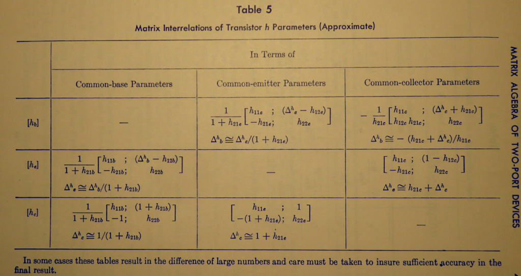
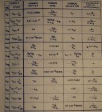
I got back to my reference books to look for the table of interrelations between h parameters for CE, CB and CC topologies.
These are not easily found. What is easy to find are tables of interrelations between various parameter types, such as Y, Z, H, ABCD, A'B'C'D' (also known as abcd), S, etc., but not between the three BJT topologies within one parameter type.
I found a good table in an old (1957) book, "Transistor Circuit Engineering" by Richard Shea.
Here is the table showing the exact conversion expressions:
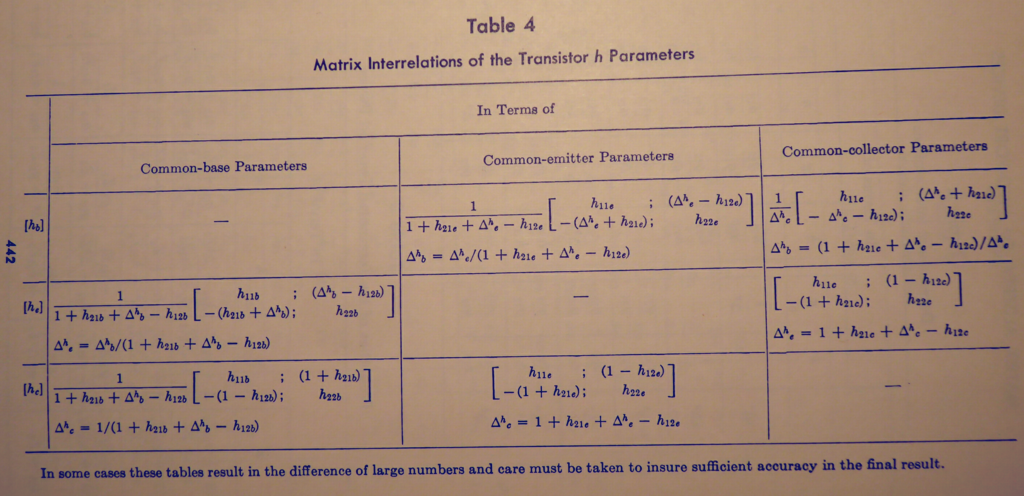
Here is the table showing approximate conversion expressions:
I've taken the CE to CB conversion matrix and rearranged it using Mathematica:
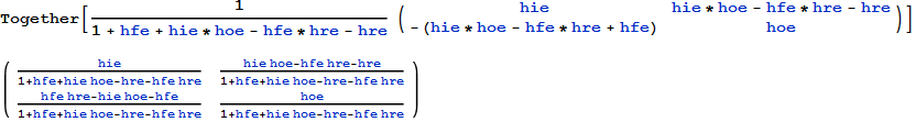
Showing it as the exact conversion from CE parameter matrix to CB parameter matrix:
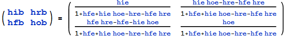
As rayfutrell mentioned in his post about writing Fortran conversion routines, some of the various conversions have the same form.
The one shown above has that property. The conversion shown converts CE parameters to CB parameters. If one just changes all the CB parameter names to CE names in the left side, and all the CE names to CB names in the right side, the result will be the exact conversion from CB to CE h parameters. In other words:
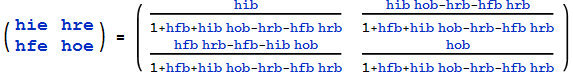
These look complicated, but I program them into my HP50G calculator. This calculator can do matrix arithmetic, so I just type a CE h parameter matrix into the calculator, press one button, and it's converted to a CB h parameter matrix. This is very handy when doing calculations with a matrix of parameters.
This is the conversion I used to convert the CE h parameters I found on the Internet to CB parameters.
Given these CE h parameters:
hie = 1200
hre = .0002
hfe = 100
hoe = .00002
Using the conversion formula we get the corresponding CB parameters:
hib = 11.881
hrb = .000037622
hfb = -.9901
hob = .00000019801
We see that hrb is not equal to hre, even approximately.
Also, hoe is much different from hob.
For these numerical values, the "exact" mub (mu of the common base topology) calculated by using the h parameter conversion to ABCD parameters, is 25001. The value of 1/hrb is 26579.9, which is a good approximation to the exact value of mub.
From the CE h parameters we get an exact value of mue of -25000, and a value of -1/hre of -5000, which is not a good approximation of mue.
These are not easily found. What is easy to find are tables of interrelations between various parameter types, such as Y, Z, H, ABCD, A'B'C'D' (also known as abcd), S, etc., but not between the three BJT topologies within one parameter type.
I found a good table in an old (1957) book, "Transistor Circuit Engineering" by Richard Shea.
Here is the table showing the exact conversion expressions:
Here is the table showing approximate conversion expressions:
I've taken the CE to CB conversion matrix and rearranged it using Mathematica:
Showing it as the exact conversion from CE parameter matrix to CB parameter matrix:
As rayfutrell mentioned in his post about writing Fortran conversion routines, some of the various conversions have the same form.
The one shown above has that property. The conversion shown converts CE parameters to CB parameters. If one just changes all the CB parameter names to CE names in the left side, and all the CE names to CB names in the right side, the result will be the exact conversion from CB to CE h parameters. In other words:
These look complicated, but I program them into my HP50G calculator. This calculator can do matrix arithmetic, so I just type a CE h parameter matrix into the calculator, press one button, and it's converted to a CB h parameter matrix. This is very handy when doing calculations with a matrix of parameters.
This is the conversion I used to convert the CE h parameters I found on the Internet to CB parameters.
Given these CE h parameters:
hie = 1200
hre = .0002
hfe = 100
hoe = .00002
Using the conversion formula we get the corresponding CB parameters:
hib = 11.881
hrb = .000037622
hfb = -.9901
hob = .00000019801
We see that hrb is not equal to hre, even approximately.
Also, hoe is much different from hob.
For these numerical values, the "exact" mub (mu of the common base topology) calculated by using the h parameter conversion to ABCD parameters, is 25001. The value of 1/hrb is 26579.9, which is a good approximation to the exact value of mub.
From the CE h parameters we get an exact value of mue of -25000, and a value of -1/hre of -5000, which is not a good approximation of mue.
Attachments


I mentioned my goal in post #1 of this thread:If Mark is looking for "maximum voltage gain", he need only find the highest Early Voltage of his PNP parts, and almost certainly find a similarly high NPN part to feed it DC without decreasing output node impedance much.
My final device selection, and my decision criteria which led to the final choice, are laid out in post #34 of this thread.I'm building current sources and current mirrors that run at about 8mA of bias, and trying to decide which device types to select. Among the criteria I have considered, is the Early Voltage (SPICE parameter "VAF"), which determines the output conductance, the "flatness" of the Ice vs Vce curves.
> how the Early Voltage of a transistor affects
It does seem odd to call a resistance a voltage.
I don't see that, James Early observed that the characteristic curves intersect at a virtual voltage (negative for NPN) and by simple trig you compute an effective output resistance. The mechanism has to do with doping densities, depletion regions, base width, etc. which are set for the intended application. Super beta transistors have very thin bases (to minimize the recombination = Ib) so collector voltage strongly effects the depletion region and VA suffers. High voltage devices have another set of trade-offs.
This exercise is useful, just as looking at quasi-saturation is useful. I assume we are trying to purpose devices for discrete audio design and the industry at large is not. Just as H&H found some medium power devices just happened to have extremely low rbb (noise). The extremely low Vcesat of these devices is not a coincidence just a result of the same device physics.
Beta-VA product is a nice figure of merit and leads to some quick rules of thumb. The 50's era horrifying maths are good to know but sometimes are too big a hammer.
If you want to win the game: cheat.
In this case, you can maximize the (Beta * Vearly) figure of merit by using a PNP transistor with infinite Beta, namely a BS250 P-channel MOSFET. It has a pretty good Vearly too: about 300 volts (!). Predictably, the standard MOS modeling equations use their own, different formulation which omits Vearly and installs Lambda instead. Ain't life grand.
In this case, you can maximize the (Beta * Vearly) figure of merit by using a PNP transistor with infinite Beta, namely a BS250 P-channel MOSFET. It has a pretty good Vearly too: about 300 volts (!). Predictably, the standard MOS modeling equations use their own, different formulation which omits Vearly and installs Lambda instead. Ain't life grand.
Attachments
Electrician,
You calculations for the conversions between the CE and CB H parameters are interesting, but you have to be careful in numerical calculations when you perform subtractions. When you subtract numbers which are almost identical, you can lose all the significant digits and further computation will be wrong. This is always a problem in computer programming. It's a big topic in the numerical analysis study of error propagation.
Robert Pease told me that Hrb=~Hre and he spent 50 years in analog circuit design. I didn't do analog circuit design so I'm taking his word for it. Mr Wurcer commented here so maybe he could shed some light on this matter.
Last edited:
Robert Pease told me that Hrb=~Hre and he spent 50 years in analog circuit design. I didn't do analog circuit design so I'm taking his word for it. Mr Wurcer commented here so maybe he could shed some light on this matter.
Trusting the difference between two large quantities as being meaningful is always a problem. What is it with the Mr.? The issues here are being overcomplicated.
...Here's a spreadsheet... And a few raw curve tracer pictures too.
Thanks for the information, I have a small query about the data.
The spreadsheet seems to be rounded to 0.05 mA but the curves appear to show better resolution than that, why the apparent inconsistency?
Best wishes
David
Electrician,
You calculations for the conversions between the CE and CB H parameters are interesting, but you have to be careful in numerical calculations when you perform subtractions. When you subtract numbers which are almost identical, you can lose all the significant digits and further computation will be wrong. This is always a problem in computer programming. It's a big topic in the numerical analysis study of error propagation.
Robert Pease told me that Hrb=~Hre and he spent 50 years in analog circuit design. I didn't do analog circuit design so I'm taking his word for it. Mr Wurcer commented here so maybe he could shed some light on this matter.
I am aware of the problems of numerical cancellation. At the very bottom of the first two images in post #51 one finds this "In some cases these tables result in the difference of large numbers and care must be taken to insure sufficient accuracy in the final result."
I did all my calculations to 15 digits and checked the individual terms in the expression for the conversion of hre to hrb. There is not a cancellation problem.
I have the utmost respect for Robert Pease, but even the most revered authority figure's assertions are subject to verification. I have now checked about 7 sets of CE h parameters, in in all cases mue is not close to -1/hre. You could check for yourself.
There seem to be two issues here. Whether 1/hre is nearly the same as 1/hrb is one. This question could be compromised by cancellation errors in the formulas for conversion from CE to CB parameters. The other issue is whether -1/hre is a good approximation to mue. This question doesn't involve CB parameters at all, and cancellation in the conversion formula isn't an issue. Using 15 digits in the H to ABCD conversion removes possibility of cancellation errors there.
I was only able to find one place where both CE and CB parameters for the same transistor are given. That was in the classic General Electric transistor manual. In the revised seventh edition can be found the following table, which unfortunately is for a germanium transistor:
The given CE h parameters are:
hie = 1400
hre = .000337
hfe = 44
hoe = .000027
Converting to CB h parameters gives:
hib = 31.1
hrb = .0005027
hfb = -.9778
hob = .0000005997
which matches the CB data in the table quite well.
Calculating mue using the H to ABCD method gives mue = -1915
Using -1/hre gives -2967, not a good approximation to -1915
Calculating mub using H to ABCD gives 1916, as expected.
Using 1/hrb gives 1989, a reasonably good approximation to 1916
Here hre is somewhat close to hrb, but the -1/hre approximation to mue doesn't work well.
Perhaps Pease was applying to specialty transistors, such as super gain BJTs. Perhaps he didn't mention it in his article because it's not as good an approximation as 1/hrb.
Attachments
Last edited:
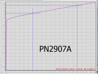
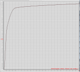
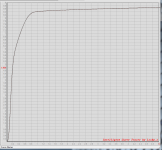
Because I read off the (I, V) datapoints by eyeballing the plots, and my eyeballs aren't infinitely precise. Take for example the PN2907A shown below.The spreadsheet seems to be rounded to 0.05 mA but the curves appear to show better resolution than that, why ... ?
My eyeballs say that at VCE=6.0, ICE = about 8.2 milliamps.
My eyeballs say that at VCE=16.0, ICE = about 9.35 milliamps.
Those are the numbers I manually typed into the spreadsheet. Then Excel calculated the slope = (9.35E-3 - 8.2E-3) / (16 - 6) = 1.15E-4 mhos. Finally Excel solved the linear equation
- slope = ICE / (VCE + Vearly)
When eyeballing the plots and typing in the data, my visual acuity may have been improved by the administration of a Glowing Pearl. Or at least, modified.
The less-than-fully-precise values of Vearly given by this informal procedure, were good enough for my purposes. If you need Vearly with greater precision, you'll need to come up with a different extraction procedure + test fixture. Or you can just use the Vearly numbers tabulated in Art Of Electronics 3rd edition, Table 8.1, page 501, and hope+trust they are correct.
_
Attachments
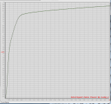
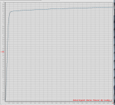
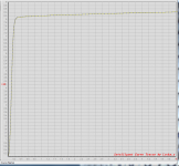
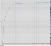
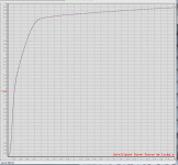
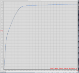
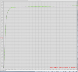
I noticed that some of the PNPs with highest Early voltage, also had an uncomfortably large "knee voltage" where the ICE vs VCE curve flattens out. So I measured the twenty highest Vearly transistors again, zoomed in around the knee voltage. Here's a table, sorted by knee voltage. 2SA1837 is (tied for) best, i.e., lowest knee voltage. MPSA92 is worst, i.e., highest knee voltage.
Hover your mouse over the image to read the filename / transistor type.
_
Hover your mouse over the image to read the filename / transistor type.
_
Attachments
-
 knee_table.png62.9 KB · Views: 288
 -
 KSA992F_Knee.PNG76.8 KB · Views: 128
 -
 KSA916Y_Knee.PNG77.8 KB · Views: 114
 -
 2SA1837_Knee.PNG83.1 KB · Views: 113
 -
 2SA1407E_Knee.PNG65 KB · Views: 113
 -
 2SA1381F_Knee.PNG89.3 KB · Views: 105
 -
 2SA970BL_Knee.PNG78.1 KB · Views: 122
 -
 2N6520_Knee.PNG92.4 KB · Views: 156
 -
 2N5401_ONS_Knee.PNG70.5 KB · Views: 268
 -
 KSA1142-O_Knee.PNG86.2 KB · Views: 124
- Home
- Amplifiers
- Solid State
- Measuring the Early voltage "VA" of some PNPs at 8mA