I've been wanting to model and simulate the BF862 JFETs I own in circuits I am considering.
In particular I wanted to understand how device variations (as characterised e.g. by different Idss) play out in a circuit.
To this end I measured the device characteristics of 14 JFETs and fitted the LTSPICE model for the saturation region.
I can model my devices fairly well by fitting 7 parameters, i.e.
VTO = -0.02280 * Idss/mA - 0.2508
beta = 0.001777 * Idss/mA + 0.02304
Rs = 0.5137 * Idss/mA - 0.5590
lambda = 0.03663
The RMS error between measured and modelled Id values is 110uA for 257 data points taken from 14 different BF862 with Idss ranging from 12.07 to 18.33mA.
For all 14 JFETs I captured Ids at Vds = 8V and Vgs= 0 .. -0.5V in 0.1V steps
For three devices (Idss = Id(Vds=8V) = 12.07, 15.17, 18.33) I took Id from Vds = 1.26V to 14V and Vgs = 0 .. -0.5V
The results I fitted for 2.5V <= Vds <= 10V using the model that LTSPICE uses for Id in the saturation region, including the effect of a finite source resistance Rs.
I used one common parameter lambda for all devices and modelled Rs, beta and VTO to depend linearly on Idss.
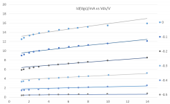
The result of the fit to the Id, Vds, Vgs array for one JFET is shown in the first attachment.
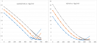
The second attachment shows measurements of the top, bottom and middle Idss JFETS in my sample of devices (Idss = 12.07, 15.17, 18.33) and the modelled Id curves for fixed Vds = 8V. The data are plotted both as sqrt(Id) and Id.
In the sqrt(Id)-plot note that the measured data are curved downward and deviate from a straight line implied by the basic JFET model. In the model this curvature is provided by finite Rs.
Also the model NXP publish for the BF862 on their website sports a Rs of 7.5 Ohm.
LTSPICE will produce the desired Id values in the saturation region when fed with only the four given parameters. However a more complete model for e.g. the Idss = 15.17mA device could be
The first four parameters are from my fitting procedure. Here you can fill in your own results depending on the Idss of your BF862.
Is and N I took as averages from Mark’s latest results.
From NXP I copied Betatce, Vtotc, Isr, Nr, Xti, Alpha, Vk, Cgd, Cgs, Kf, Af.
I ditched Rd, because I don’t model it explicitly so the effect of a finite drain resistance is folded into the model results.
I also ditched M because I couldn’t find out what it does.
Feel free to make your own choices for the extra parameters, they don’t affect Id in the saturation region (if you don’t tamper with the temperature).
Edit: as per keantoken's hint you can adapt your ltspice simulations to the Idss of your devices simply by using your favorite BF862 model (e.g. the one above) and then altering it via
That way you can even .step through different devices.
In particular I wanted to understand how device variations (as characterised e.g. by different Idss) play out in a circuit.
To this end I measured the device characteristics of 14 JFETs and fitted the LTSPICE model for the saturation region.
I can model my devices fairly well by fitting 7 parameters, i.e.
VTO = -0.02280 * Idss/mA - 0.2508
beta = 0.001777 * Idss/mA + 0.02304
Rs = 0.5137 * Idss/mA - 0.5590
lambda = 0.03663
The RMS error between measured and modelled Id values is 110uA for 257 data points taken from 14 different BF862 with Idss ranging from 12.07 to 18.33mA.
For all 14 JFETs I captured Ids at Vds = 8V and Vgs= 0 .. -0.5V in 0.1V steps
For three devices (Idss = Id(Vds=8V) = 12.07, 15.17, 18.33) I took Id from Vds = 1.26V to 14V and Vgs = 0 .. -0.5V
The results I fitted for 2.5V <= Vds <= 10V using the model that LTSPICE uses for Id in the saturation region, including the effect of a finite source resistance Rs.
I used one common parameter lambda for all devices and modelled Rs, beta and VTO to depend linearly on Idss.
The result of the fit to the Id, Vds, Vgs array for one JFET is shown in the first attachment.
The second attachment shows measurements of the top, bottom and middle Idss JFETS in my sample of devices (Idss = 12.07, 15.17, 18.33) and the modelled Id curves for fixed Vds = 8V. The data are plotted both as sqrt(Id) and Id.
In the sqrt(Id)-plot note that the measured data are curved downward and deviate from a straight line implied by the basic JFET model. In the model this curvature is provided by finite Rs.
Also the model NXP publish for the BF862 on their website sports a Rs of 7.5 Ohm.
LTSPICE will produce the desired Id values in the saturation region when fed with only the four given parameters. However a more complete model for e.g. the Idss = 15.17mA device could be
Code:
.model BF862-13 NJF(
+ beta= 0.049998 VTO= -0.5967 lambda= 0.036629 Rs= 7.234
+ Is= 9.36E-14 N= 1.245
+ Betatce=-.5 Vtotc=-2.0E-3 Isr=2.995p Nr=2 Xti=3 Alpha=-1.0E-3
+ Vk=59.97 Cgd=7.4002E-12 Pb=.5 Fc=.5 Cgs=8.2890E-12 Kf=87.5E-18 Af=1)
* Idss:15.2Is and N I took as averages from Mark’s latest results.
From NXP I copied Betatce, Vtotc, Isr, Nr, Xti, Alpha, Vk, Cgd, Cgs, Kf, Af.
I ditched Rd, because I don’t model it explicitly so the effect of a finite drain resistance is folded into the model results.
I also ditched M because I couldn’t find out what it does.
Feel free to make your own choices for the extra parameters, they don’t affect Id in the saturation region (if you don’t tamper with the temperature).
Edit: as per keantoken's hint you can adapt your ltspice simulations to the Idss of your devices simply by using your favorite BF862 model (e.g. the one above) and then altering it via
Code:
.param Idss = 15
.model BF862Idss ako:BF862 beta={0.001777*Idss+0.02304} VTO={-0.0228*Idss-0.2508} Rs={0.5137*Idss-0.559}Attachments
Last edited:
Rs = 0.5
If you feel that Rs shouldn’t be device specific and rather a constant of 0.5 established by a different experiment the fit naturally gets worse.
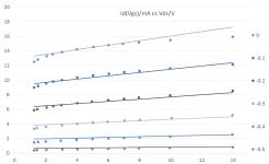
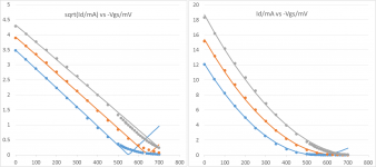
The first and second attachments in this post show the resulting fit to the same (Id, Vds, Vgs) arrays as before.
RMS error is 185uA.
The coefficients to derive beta and VTO from Idss in this setting are given as
beta = -0.0007956 * Idss/mA + 0.04376
VTO = -0.03038 * Idss/mA - 0.1840
with
lambda = 0.02524
Rs = 0.5
If you feel that Rs shouldn’t be device specific and rather a constant of 0.5 established by a different experiment the fit naturally gets worse.
The first and second attachments in this post show the resulting fit to the same (Id, Vds, Vgs) arrays as before.
RMS error is 185uA.
The coefficients to derive beta and VTO from Idss in this setting are given as
beta = -0.0007956 * Idss/mA + 0.04376
VTO = -0.03038 * Idss/mA - 0.1840
with
lambda = 0.02524
Rs = 0.5
Attachments
Useful info:
I think the BF862 is a symmetrical chip (common for FETs). This is because when I first used them I accidentally had the source and drain swapped - when I fixed it they behaved exactly the same, same Vgs.
So I think based on this Rd should = Rs
EDIT: I notice Rd is not the same as Rs for the NXP model. For the BF861 models they are equal. Hmm.
Last edited:
I think the BF862 is a symmetrical chip (common for FETs). This is because when I first used them I accidentally had the source and drain swapped - when I fixed it they behaved exactly the same, same Vgs.
NXP says so in the data sheet, directly on the top.
BTW The discrete parts division that makes the BF862 has just been sold
to a Chinese company. Maybe I should get me a reel.
I just soldered 16 FETs on a new measurement preamp board that was delivered
on Friday.
")
Somewhere I read that parts made in Hong Kong had a better 1/f corner than
those from mainland China. These 100+100 I got from Digikey & Mouser
last week are all marked 2AW, which would mean higher 1/f.
regards, Gerhard
Useful info:
I think the BF862 is a symmetrical chip (common for FETs). This is because when I first used them I accidentally had the source and drain swapped - when I fixed it they behaved exactly the same, same Vgs.
So I think based on this Rd should = Rs
EDIT: I notice Rd is not the same as Rs for the NXP model. For the BF861 models they are equal. Hmm.
yup, data sheet says its symmetrical.
The point with Rs here is that IMHO it is not a physical quantity like the bonding wire resistance inside the package. It is a fitting parameter that helps to bend the sqrt(Id) curves to match the data. And it works very well...
Could you show how well these match the fitted VTO, BETA, and RS of your three devices (Idss = Id(Vds=8V) = 12.07, 15.17, 18.33) ?VTO = -0.02280 * Idss/mA - 0.2508
beta = 0.001777 * Idss/mA + 0.02304
Rs = 0.5137 * Idss/mA - 0.5590
Since these equations have two degrees of freedom (slope + intercept), fitting them to only three datapoints probably gives a close match; but it would be reassuring to see the actual data nevertheless.
Not sure what you are asking for.
I fit 7 parameters to 257 data points from 14 devices.
For the three mentioned I have data of various Vds. All others are only taken at Vds = 8V.
So I don't fit VTO, Beta, Rs by device, I fit coefficients for those parameters for all devices.
And its one big ole nasty fit for all data.
I fit 7 parameters to 257 data points from 14 devices.
For the three mentioned I have data of various Vds. All others are only taken at Vds = 8V.
So I don't fit VTO, Beta, Rs by device, I fit coefficients for those parameters for all devices.
And its one big ole nasty fit for all data.
Thanks for explaining, I think I understand. It would be reassuring to see the measured-vs-spicemodel data for two of those 14 devices: (i) the device with the largest positive difference between measured and modeled; (ii) the device with the largest negative difference between measured and modeled.
Of course this might open a can of worms: how do you define "difference" i.e. "error"? Is it (measured-modeled)^2 ? Is it |measured-modeled| ? Is it ((measured-modeled)/measured)^2 ? etc. Each of these are reasonable choices and there are other reasonable choices too. But however you have chosen to define fitting error, there exists two devices with the greatest error, and people considering adopting your models are probably interested to know "how bad can it get"?
Of course this might open a can of worms: how do you define "difference" i.e. "error"? Is it (measured-modeled)^2 ? Is it |measured-modeled| ? Is it ((measured-modeled)/measured)^2 ? etc. Each of these are reasonable choices and there are other reasonable choices too. But however you have chosen to define fitting error, there exists two devices with the greatest error, and people considering adopting your models are probably interested to know "how bad can it get"?
yup, data sheet says its symmetrical.
The point with Rs here is that IMHO it is not a physical quantity like the bonding wire resistance
That would be .1 Ohm or so anyway. As long as the fitting does not affect the noise I don't see a problem with it being a few Ohms off from reality. It is very difficult to measure since the parasitic gate resistance is not 0 either. Has anyone tried the impact ionization in LTSPICE compared to reality?
Last edited:
Could you show how well these match the fitted VTO, BETA, and RS of your three devices (Idss = Id(Vds=8V) = 12.07, 15.17, 18.33) ?
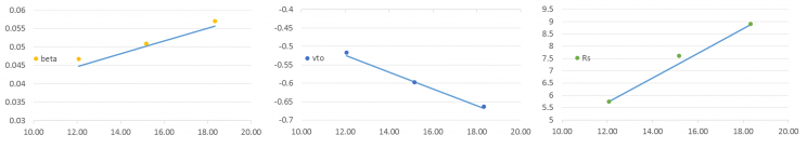
Since you asked so nicely here are the parameters for individual fits to the data of each of the three devices (still common lambda).
Points are individual fits, lines are the linear relationships for all data as cited above. All shown over Idss/mA.
Attachments
the parasitic gate resistance is not 0 either.
When I measured the BF862 gate-to-source junction diode in forward bias, below 10 mA datasheet abs max rating, the plot deviated from pure semilog behavior enough to extract a series resistance term (I estimate it's only good to 1 significant figure).
You could do this for gate-to-source with drain floating, then do it again for gate-to-drain with source floating, then do it again for gate-to-source-and-drain where D+S are shorted. These measurements give three resistances, which after a little algebra become Rgate, Rsource, and Rdrain. They're the sum of all DC resistances: test fixture + package lead + bondwire + on-die metallization + sheet resistance of N+ or P+ region + ... etc. I estimate they'll probably only be good for half a significant figure, i.e., plus or minus 32 percent (0.1^0.5). But it's better than nothing.
Thanks for explaining, I think I understand. It would be reassuring to see the measured-vs-spicemodel data for two of those 14 devices: (i) the device with the largest positive difference between measured and modeled; (ii) the device with the largest negative difference between measured and modeled.
Of course this might open a can of worms: how do you define "difference" i.e. "error"? Is it (measured-modeled)^2 ? Is it |measured-modeled| ? Is it ((measured-modeled)/measured)^2 ? etc. Each of these are reasonable choices and there are other reasonable choices too. But however you have chosen to define fitting error, there exists two devices with the greatest error, and people considering adopting your models are probably interested to know "how bad can it get"?
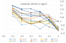
I can show you the residuals for the Vds = 8V data, so you can have a look "how bad it can get". And I chose (measured-modeled)^2 as you surely already guessed from the RMS error given in uA.
Attachments
BF862 models by Idss
For simulating the impact of device variations I determined one spice model per tenth of a mA and put them in a file.
Each model is labelled BF862-xx.x where xx.x is the Idss value in mA with one figure after the decimal point.
Have fun.
For simulating the impact of device variations I determined one spice model per tenth of a mA and put them in a file.
Each model is labelled BF862-xx.x where xx.x is the Idss value in mA with one figure after the decimal point.
Have fun.
Attachments
Wow, thanks. I think you should be able to step through the values using a .param and .step scheme.
That would be fun. Do you know how to do this in LTspice?
Nice!
Where does one find such statements like AKO:{}?
A word of warning about the models, still.
Please look at the first post how I derived them. They are not meant to exactly reproduce Idss but to give the best fit over the given range of Vds/Vgs values.
They do recover Idss within +-0.1mA for Idss = 10 .. 20mA, though.
OK, found it:
Undocumented LTspice - LTwiki-Wiki for LTspice
towards the end of the page: AKO Aliases (A Kind Of)
In that case you can also forget the file and do it like this.
Undocumented LTspice - LTwiki-Wiki for LTspice
towards the end of the page: AKO Aliases (A Kind Of)
In that case you can also forget the file and do it like this.
Attachments
Yep, that is a saner way to do it, if you have equations for the parameters that get changed. Much better than cycling through a list.
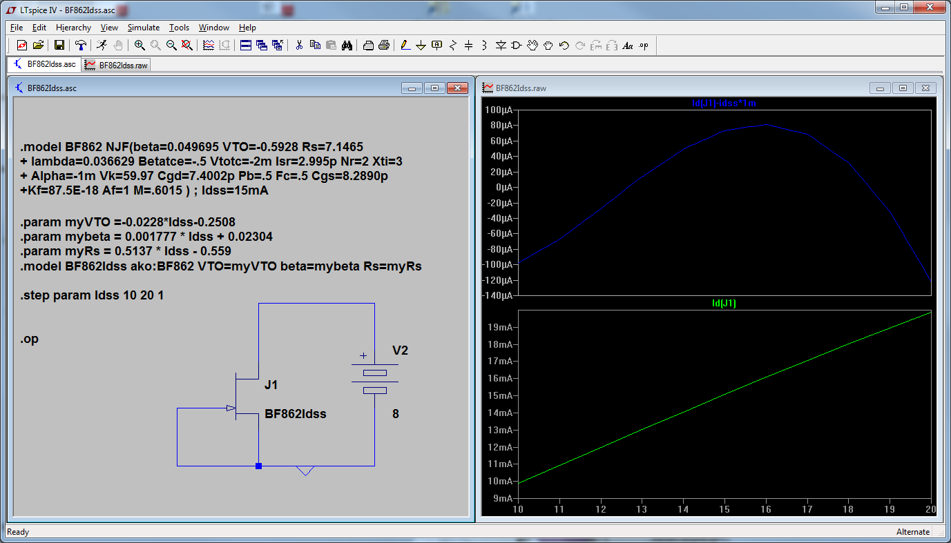
The equations can be put in the model or AKO model using curly brackets:
.model BF862 NJF(beta=0.049695 VTO=-0.5928 Rs=7.1465
+ lambda=0.036629 Betatce=-.5 Vtotc=-2m Isr=2.995p Nr=2 Xti=3
+ Alpha=-1m Vk=59.97 Cgd=7.4002p Pb=.5 Fc=.5 Cgs=8.2890p
+Kf=87.5E-18 Af=1 M=.6015 ) ; Idss=15mA
.model BF862Idss ako:BF862 beta={0.001777*Idss+0.02304} VTO={-0.0228*Idss-0.2508} Rs={0.5137*Idss-0.559}
If you put this in your standard.jft or .lib/.inc it, LTspice may complain if you do not have the IDSS parameter specified on your schematic.
- Status
- This old topic is closed. If you want to reopen this topic, contact a moderator using the "Report Post" button.
- Home
- Amplifiers
- Solid State
- LTSPICE model for your BF862 JFETs