I am not SMD intergrist, i use them where they let me win place or shorter electrical travel. As my board are home etchable and single layer they can not be exclusiv SMD as tracks run under classical through. As i build several differents electonic stuffs the 100 u are not lost and even i would buy 10 form value i local shop it will coast same avrage as 100 from where i buy them actualy. Take a look at TME online shop for europe buyeur. These shop is in Poland and deliver in france next day for about 8€ without minimun order. Really good shop.
Marc
Marc
Alternative Q3 to Q6.
Hi Pete,
i refer you to post 65.
Regarding Q3 ,4 ---KSA 1381 E and KSC 3503E --can i replace with BD140 and 139?
Q5, Q6--2Sk 1058, 2sj 162--can i replace with IRFP 9240 and 240 ??
Q11, 12 , the J112 replaced with 2n3819
I have these parts left over from other projects>
thanks
kp93300
Hi Pete,
i refer you to post 65.
Regarding Q3 ,4 ---KSA 1381 E and KSC 3503E --can i replace with BD140 and 139?
Q5, Q6--2Sk 1058, 2sj 162--can i replace with IRFP 9240 and 240 ??
Q11, 12 , the J112 replaced with 2n3819
I have these parts left over from other projects>
thanks
kp93300
Hi Pete,
i refer you to post 65.
Regarding Q3 ,4 ---KSA 1381 E and KSC 3503E --can i replace with BD140 and 139?
Q5, Q6--2Sk 1058, 2sj 162--can i replace with IRFP 9240 and 240 ??
Q11, 12 , the J112 replaced with 2n3819
I have these parts left over from other projects>
thanks
kp93300
Hi,
2SK1058/2SJ162 are lateral Fet and IRFP240/9240 are vertical FET...so not direct compatible...
Marc
Not optimal, but yes, and only up to +/-40V supply, not to be exceeded, and best to stay under 38V, in this case. I plan to supply the KSA1381E and KSC3503E to as many people as want to use them.Hi Pete,
i refer you to post 65.
Regarding Q3 ,4 ---KSA 1381 E and KSC 3503E --can i replace with BD140 and 139?
No, answered above by Marc.Q5, Q6--2Sk 1058, 2sj 162--can i replace with IRFP 9240 and 240 ??
Yes, but note that the J112 will be supplied with the boards.Q11, 12 , the J112 replaced with 2n3819
I have these parts left over from other projects>
thanks
[/QUOTE]
Q11/Q12 Component Numbering
For anyone else -
I apologize for the transistor numbering running up to 12. It happened when I was trying symbols with different footprints, and I forgot to reset the Q11 and Q12 component names.
There are no undocumented or hidden parts...
There are only six transistors in the actual amplifier circuit, plus the two Jfets currently numbered Q11 and Q12. So, the numbers should have run from 1 to 8.
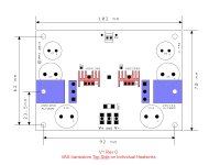
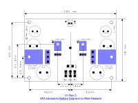
Dimensions & Mounting Holes
Outside dimensions of the circuit board are 102 x 70 mm (4"x2.75"). When the circuit board is vertically centered on a typical heatsink with external fins, the power devices will be offset toward the bottom for better thermal management. Ideal position would be with the latfet mounting screws 40~45% of the heatsing height from the bottom, and 55~60% from the top.
There are 8 mounting holes, most of them optional. The circuit board is stable, even if only atached to the heatsink using the two Latfet mounting screws.
Two aditional M3 screws can be used for added support. Not more than 4 total recommended, because alignment becomes more difficult with each additional pair. Two examples are shown below.
For best results, the version with the VAS heatsinks should be mounted so that warm air can rise up toward the top of the chassis without obstruction or heating the electrolytic caps. The version with VAS transistors on the main heatsink can be rotated 180 degrees if more convenient.
First Pic, VAS transistor top-side
Latfets: Blue hilite
VAS top-side: Red hilite, including VAS heatsinks
Second Pic, VAS transistors bottom
Latfets: Blue hilite
VAS bottom-side: Blue hilite, mounted on main heatsink.
Attachments
The board does actually have a CRC filter for the front end. The rails are split by a diode-resistor circuit, so at the front end, it looks like C-DR-C.PMI, could you consider provisions for a couple of 35mm diameter bulk filter caps, and perhaps resistor locations also, for those who prefer the simplicity of an onboard CRC supply?
Not sure whether that would adversely effect board size and layout.
Making a bigger board with CM or CRC filters is more difficult/expensive, because the discounts I take advantage of to get the first one or two orders do not apply when the square area gets bigger. Manufacturers put extra boards on unused panel space (a typical panel is 12x18 inches) from larger orders to run small lots. When the board gets to a certain size, or shape, that no longer works.
It could still be done. The layout can be tested with just the amp circuit, and then enlarged for the filter caps before a 100-piece~250 piece order. Less than 100 units, cost for one board would be high.
Hi PMI
Looking at your schematics it looks like the output bias is function of the VAS current when adjusted with the CCS potentiometers. Indeed, the VGSoff of the lateral MOSFET has a wide spreading...There is no pot for R19. Is that on purpose?
You may want the Zener Z1 and Z2 to kick in before the internal diodes of the mosfets by selecting a lower voltage value. This way you can save the MOSFET in case of a fault like a short circuit or else...
I suppose that most peoples will not use C1 if they have a low DC offset preamp...
Why the 1000uf caps for the output are different than the ones for the front end?
For the feedback resistors if peoples sometimes use expensive caddock for other amps, for this one I would either use a higher power one or a very low temp coefficient and probably both...
Thanks
Fab
Last edited:
Thanks PMI, that's good to know and answers my question. Is it viable to negate the need for a separate power supply board by increasing the value of the existing 4x onboard filter caps and complementing them with a couple of off-board screw caps to take up the ripple? Which brings me to my next question... what is the largest diameter cap the board will hold?
I'll probably build this with another of your cap multi boards anyway, but flexibily is always good.
The height of the board is perfect for a 75mm Conrad heatsink, which in turn fits nicely inside 2U cases. MOSFET positioning for optimal thermal dissipation is a nice touch.
My only other suggestion is whether the board can be made slightly narrower (say 98mm) so that two boards could be mounted side-by-side on a single 200mm heatsink? Alternatively could the MOSFETs be mounted slightly further inboard, towards the centre-line to achieve the same result?
Its not a big issue and I suspect most constructors will either use two heatsinks flanking the left and right hand sides of the chassis, or a single heatsink > 200mm. It would benefit constructors like myself who prefer to use a single heatsink mounted inside the case where space is limited.
On purpose, yes. I wanted to avoid a third trim pot. The output bias and VAS bias can be adjusted to what LazyCat recommended +/- a good margin, with just the two trim pots. My test boards are adjsuted to 160 mA, with about 13~18 mA VAS bias, depending on supply voltage. Slightly higher than original VSSA. Offset is adjusted with the same two trim pots, without changing the bias. The trim pots are antagonistic for bias, and complementary (with bias constant) for offset.Hi PMI
Looking at your schematics it looks like the output bias is function of the VAS current when adjusted with the CCS potentiometers. Indeed, the VGSoff of the lateral MOSFET has a wide spreading...There is no pot for R19. Is that on purpose?
For normal listening, up to 35V supply, a higher power resistor is not required. Demand for high power is transient. However, there is some benefit from using 50 ppm resistors, which are available from Mouser for only pennies more.
Over 45V, the power rating should be increased. For some of my testing at continuous higher power, I am using Vichay/Dale CPF series 2K21 1W feedback resistors, which fit a 10-mm hole spacing. This unfortunately means that for best results, the 100R should be the same type...
Between 35 and 45V it is a toss-up.
The same 1000uF caps can be used for output and front end. Mine are different because I like to use caps with a high ripple rating and low series resistance at the output. At the front end, where current demand is less, I decided to use the caps LC recommended, Nichicon FG series.
Probably not, sorry.Is it viable to negate the need for a separate power supply board by increasing the value of the existing 4x onboard filter caps and complementing them with a couple of off-board screw caps to take up the ripple? Which brings me to my next question... what is the largest diameter cap the board will hold?
The boards can be made narrower, but a single heatsink may get a bit warm...
Mosfets can be moved in, toward the center of the board, but at the cost of some lost space for the VAS heatsinks.18-mm diameter caps will fit, but just barely. 16-mm should be considered typical. Some room could be made to fit 18-mm better, but if I increase it to 18-mm, someone will just ask for 20-mm, that is just human nature, regardless of actual need.
The CM PSU was originally intended for this board, but there was a "small delay",I'll probably build this with another of your cap multi boards anyway, but flexibily is always good.
edit:
I should have added that I would not have thought that a single 200-mm heatsink was even an option. If you think it is, perhaps this is something that should be changed (?)
Last edited:
Hi PMI
Your boards are so nice that I could use them to replace my own original version of the now called VSSA. My version was made with a generic modified F5 pcb(from EBAy) for the front end and an old prototype board for output stage (3pairs) since no pcb existed at the time (in spring 2012)...
Please count me in for 2 boards.
Thanks again to share that with us !
Fab
Hi PMI,
I'll do like Fab and get two boards please.
Ciao!
Do
On purpose, yes. I wanted to avoid a third trim pot. The output bias and VAS bias can be adjusted to what LazyCat recommended +/- a good margin, with just the two trim pots. My test boards are adjsuted to 160 mA, with about 13~18 mA VAS bias, depending on supply voltage. Slightly higher than original VSSA. Offset is adjusted with the same two trim pots, without changing the bias. The trim pots are antagonistic for bias, and complementary (with bias constant) for offset.
For normal listening, up to 35V supply, a higher power resistor is not required. Demand for high power is transient. However, there is some benefit from using 50 ppm resistors, which are available from Mouser for only pennies more.
Over 45V, the power rating should be increased. For some of my testing at continuous higher power, I am using Vichay/Dale CPF series 2K21 1W feedback resistors, which fit a 10-mm hole spacing. This unfortunately means that for best results, the 100R should be the same type...
Between 35 and 45V it is a toss-up.
The same 1000uF caps can be used for output and front end. Mine are different because I like to use caps with a high ripple rating and low series resistance at the output. At the front end, where current demand is less, I decided to use the caps LC recommended, Nichicon FG series.
Hi PMI
Have you determined the min and max of the VAS current to cover the whole VGS threshold range of the lateral ( for the 160 ma) in your 13-18 ma number ? And if we want higher output bias? One way would be to specify a resistor value for R19 based on desired output bias....
For the feedback resistors I was not referring to the power handling but to the value thermal drift and for sure 50 ppm per C is a good choice. But it is the C of the resistor that I want to reduce by bigger resistor body or property...
For the cap types it makes a lot of sense.
If you have terminal tabs at R11/12 you can connect and use a separate regulated supply for the front end of the amp and not connect R12/12 and diodes....
Thanks
Fab
Last edited:
No I have not (if I understand the question). I was mostly concerned about having enough adjustment range to set the output bias where I wanted it, and how the setting changed at different supply voltages.Have you determined the min and max of the VAS current to cover the whole VGS threshold range of the lateral ( for the 160 ma) in your 13-18 ma number ?
Yes. I think someone suggested putting three diodes in series instead of two... to be honest, it worked so well as originally specified by Lazy Cat, and later modified by Shaan for the Renesas latfets, I did not experiment with the output bias much at that time. We can certainly try it...And if we want higher output bias? One way would be to specify a resistor value for R19 based on desired output bias....
In a practical amp there is more to be gained from lower thermal drift than from higher power rating. (For testing, I need the 1W because I want to be able to run continuous higher power sine and square waves.) I will take this to a separate post...For the feedback resistors I was not referring to the power handling but to the value thermal drift and for sure 50 ppm per C is a good choice. But it is the C of the resistor that I want to reduce by bigger resistor body or property...
Yes, and I think it would be good to talk about the supply to the front end in general.If you have terminal tabs at R11/12 you can connect and use a separate regulated supply for the front end of the amp and not connect R12/12 and diodes....
Do you think there is something to be gained from having an option for a completely separate front-end supply? I ask because -
In the main VSSA thread, the latest recommendation is to eliminate (short with a jumper) the series DR completely (!) A couple people report an improvement in sound, specifically in Bass by doing this. So this would seem to be opposite from a separate supply.
Personally I do not see much use for the diode, unless you have a very poor supply (tested). However, I think I would keep the resistor.
Also, if I expand the footprint for the main decoupling cap so 18 mm is a good fit, instead of a tight fit, AND tabs for a separate front end supply, I cannot at the same time shrink the board by 2 mm as suggested above....
Feedback Resistors, continued...
Lower temp coefficient: The easiest improvement is 50 ppm, which cost only pennies more. Example, Xicon 271-2.2K, 1/4W, 50ppm, ~10 cents.
Larger body and therefore bigger surface area: Vishay/Dale RN60/CMF60) series, almost 4-mm in diameter, and with very good specs for low noise, and low drift. Especially suitable for a feedback resistor because the voltage coefficient is vanishingly small. In other words, the value will not change over a wide range of feedback voltage. The RN60 1/4W is the equivalent of a commercial CMF60 rated at 1W/70C, and biggest bang for the buck, because it actually costs much less than the commercial version, about 20 cents each, (some values less). Pins have to bent in about 1/2 mm for a good fit on the current layout. Example, RN60D2201.
Higher Power in same size as 1/4W: Vishay Dale CPF1 series. Same low noise and low voltage coefficient specs as the RN60 series, 1W rating in a 1/4W size. Unfortunately most expensive, 30~50 cents each. Example, CPF12K2100.
At normal listening power levels, a 1/4W 2.2K 100 ppm is probably sufficient, but some improvements can probably be made by selecting lower ppm, or higher power, resistors, or parts with bigger surface area, depending on what you want to achieve.For the feedback resistors I was not referring to the power handling but to the value thermal drift and for sure 50 ppm per C is a good choice. But it is the C of the resistor that I want to reduce by bigger resistor body or property...
Lower temp coefficient: The easiest improvement is 50 ppm, which cost only pennies more. Example, Xicon 271-2.2K, 1/4W, 50ppm, ~10 cents.
Larger body and therefore bigger surface area: Vishay/Dale RN60/CMF60) series, almost 4-mm in diameter, and with very good specs for low noise, and low drift. Especially suitable for a feedback resistor because the voltage coefficient is vanishingly small. In other words, the value will not change over a wide range of feedback voltage. The RN60 1/4W is the equivalent of a commercial CMF60 rated at 1W/70C, and biggest bang for the buck, because it actually costs much less than the commercial version, about 20 cents each, (some values less). Pins have to bent in about 1/2 mm for a good fit on the current layout. Example, RN60D2201.
Higher Power in same size as 1/4W: Vishay Dale CPF1 series. Same low noise and low voltage coefficient specs as the RN60 series, 1W rating in a 1/4W size. Unfortunately most expensive, 30~50 cents each. Example, CPF12K2100.
- Status
- This old topic is closed. If you want to reopen this topic, contact a moderator using the "Report Post" button.
- Home
- Amplifiers
- Solid State
- VSSA Through-Hole-PCB build thread