Don't get me wrong here, I'm not suggesting that the dual die Exicons would be the preferred device, just that it could be a pretty capable little beast with them. To the contrary, I'm still very much on board with the original concept.
There was some very early interest in paralleled devices and it seems perhaps a logical step to take. Also, the idea of using a bootstrap arrangement can make the amp a little more voltage efficient.
I'll post my current idea shortly.
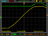
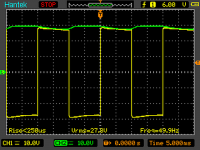
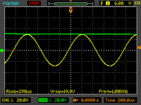
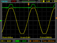
I have made the bootstrapped version already, I used 1k resistor and 100uF cap (47uF should be fine too). It sound really OK.
I found that double bootstrap separated with diode is increasing slightly thd (measurements done on fet-hex thred), better version would be standart with two high power rated (3W-5W) resistors, than we should have some extra heat but unchanged thd.
Attachments
I not often bougth heatsink as i have good rubish findings
My Nmos 200 : each heatsink mesure 230x200x40mm with 10mm base plate rated 0.4K/W and have 6 more

My NBip : each heatsink mesure 265x150x75mm with more than 10mm base plate rated around 0.2-0.25K/W and have 3 more
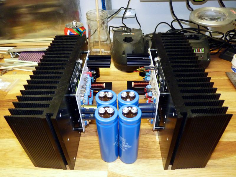
I have found some more others :
- 5u 300x75x40mm rated 0.45K/W
- 3u 300x120x40mm rated 0.4K/W
My Nmos 200 : each heatsink mesure 230x200x40mm with 10mm base plate rated 0.4K/W and have 6 more
My NBip : each heatsink mesure 265x150x75mm with more than 10mm base plate rated around 0.2-0.25K/W and have 3 more
I have found some more others :
- 5u 300x75x40mm rated 0.45K/W
- 3u 300x120x40mm rated 0.4K/W
@Idefixes:  anytime you can recycle anything and keep it out of the landfill, it is a win in my book!
The first version of my chassis was made almost completely with parts from the scrap bucket at a local machine shop, although I DID have to buy the heatsinks...
The next couple I have to pay for, since finding identical scrap parts is hard (chuckle). I plan to make around six similar to that one, and perhaps standard width, with the same heatsinks from Heatsink USA, one of the companies that is supporting us with their advertising here..
Btw, Heatsink USA does advertise that they will machine parts to order.
anytime you can recycle anything and keep it out of the landfill, it is a win in my book! The first version of my chassis was made almost completely with parts from the scrap bucket at a local machine shop, although I DID have to buy the heatsinks...
The next couple I have to pay for, since finding identical scrap parts is hard (chuckle). I plan to make around six similar to that one, and perhaps standard width, with the same heatsinks from Heatsink USA, one of the companies that is supporting us with their advertising here..
Btw, Heatsink USA does advertise that they will machine parts to order.
double output

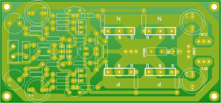
Progress so far:-
Re-aligned some resistors/diodes.
Added larger electro caps for supply decouple.
Added compensation caps.
Now making the silkscreen(see attachment). Is this silk style cool or should I follow some other style?
shaan
Progress so far:-
Re-aligned some resistors/diodes.
Added larger electro caps for supply decouple.
Added compensation caps.
Now making the silkscreen(see attachment). Is this silk style cool or should I follow some other style?
shaan
Attachments
hi Shaan, it's nice layout with big elco supply i'll use panasonic fc 1000uf/50v.
Progress so far:-
Re-aligned some resistors/diodes.
Added larger electro caps for supply decouple.
Added compensation caps.
Now making the silkscreen(see attachment). Is this silk style cool or should I follow some other style?
shaan
if 10uf mkp/mkt will be used for input, i think it's too small pattern.
Progress so far:-
Re-aligned some resistors/diodes.
Added larger electro caps for supply decouple.
Added compensation caps.
Now making the silkscreen(see attachment). Is this silk style cool or should I follow some other style?
shaan
Looks cool.
My 2cents - if you are using multiple pairs of outputs I would recommend source resistors anyway, and by adding only 3 small elements per rail you are getting around 35W more - from the same psu.
...if 10uf mkp/mkt will be used for input, i think it's too small pattern.
What is the lead spacing of the MKT?
Looks cool.
Thanks.
...if you are using multiple pairs of outputs I would recommend source resistors anyway.
Why? The 1ohm RDSon of the laterals can't force current sharing? Besides, I'm afraid of putting inductive elements in the source node, can create mysterious problems.
...by adding only 3 small elements per rail you are getting around 35W more - from the same psu.
Haven't tested this myself so it may be added to a later version of the board when I do. I would request fellows to try the config with bootstrap and laterals themselves before publishing a design for it.
Shaan,What is the lead spacing of the MKT?
I got 27.5mm lead spacing for same brand 1uF that u use...
this one 10uF/100v
on the right is the black one
but we can always use multiple holes
Attachments
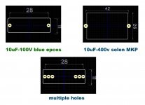
Max dim w/ Multi hole is better way to go....
Absolutely!
@shaan: Some component-to-component spacing looks very close. It is workable, but could be a bit wider.
The pin of the gate resistor which is closest to the edge of the board seems a bit close to the body of the mosfet, under the board. You can create a pcb symbol for the mosfet which includes the silkscreen for horizontal outline. This also helps when you run the design check in the layout program.
The pins of the resistors which are closest to the bottom side of the VAS transistor seem too close to where a small heatsink would mount, if at the board level. Dual mosfets usually means higher supply voltage at the VAS transistor, so assuming the same bias current, more heat dissipation (I think about 30% more?). With the small-ish heatsink I am using, the temperature rise at the case of the VAS transistor on my board is around 20-25C at idle, and goes up from there.
Some of the elcos people are likely to use for the rail caps may have 1-mm pin size, so that means a bigger hole. This also applies to the diode which splits the rail at the VAS supply point, the diode would usually have a thicker lead diameter than the associated 10R.
Btw, the 10u film cap LC has used on his modules is 15-mm lead spacing.
@shaan: Some component-to-component spacing looks very close. It is workable, but could be a bit wider.
The FET's body isn't supposed to be in contact with the underside of the board; there will be no hole on the board for fixing the FETs. Both the N and P channel FETs will have their holes outside the board area, with say, 3-5mm gap between the them and the board. I did it this way coz otherwise the board length and width will have to be increased even more.
The pins of the resistors which are closest to the bottom side of the VAS transistor seem too close to where a small heatsink would mount, if at the board level. Dual mosfets usually means higher supply voltage at the VAS transistor, so assuming the same bias current, more heat dissipation (I think about 30% more?). With the small-ish heatsink I am using, the temperature rise at the case of the VAS transistor on my board is around 20-25C at idle, and goes up from there.
Some of the elcos people are likely to use for the rail caps may have 1-mm pin size, so that means a bigger hole. This also applies to the diode which splits the rail at the VAS supply point, the diode would usually have a thicker lead diameter than the associated 10R.
Btw, the 10u film cap LC has used on his modules is 15-mm lead spacing.
Thanks for the tips Pete. The spacing and hole diameter will be taken care of.
I am also thinking of splitting the circular ground trace near the input node, With two 10R resistors in series from upper trace to the lower, and then supply the input ground reference(0V in) and bias(10K) from the two resistor's junction. How does this sound? One can always short the resistors with jumpers if necessary.
For the input ground reference, I think that is a good idea.Thanks for the tips Pete. The spacing and hole diameter will be taken care of.
I am also thinking of splitting the circular ground trace near the input node, With two 10R resistors in series from upper trace to the lower, and then supply the input ground reference(0V in) and bias(10K) from the two resistor's junction. How does this sound? One can always short the resistors with jumpers if necessary.
I have to think about the bias ground.
In some other applications I am familiar with, a ground trace which circles the board can (although not necessarily will) cause some issues which then have to be overcome in other ways. What I am referring to is that as the load shifts from one rail to the other, an alternating current is generated in what is essentially a loop, and a loop antenna. The current reverses direction when the output signal crosses zero. So if you bring a small signal on a pair of wires close to that without additional shielding, there may be an issue. (note that I say "may", not will).
So splitting the ground trace in whatever way would help with that too, I think.
- Home
- Amplifiers
- Solid State
- PeeCeeBee