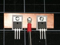
The leads of the mosfets look like they are bent very close to the plastic case. According to the TO-3P drawing, it seems you need 2 mm plus the bend radius (?)No comments?
The leads of the mosfets look like they are bent very close to the plastic case. According to the TO-3P drawing, it seems you need 2 mm plus the bend radius (?)
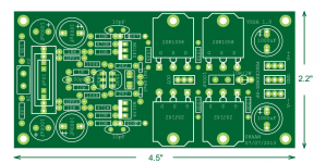
Now we have 5mm. Board dimensions: 4.5" x 2.2"
Attachments
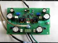
... At some point you may want to post some directions on the correct steps to align, mount, and solder two rows of devices...
I agree, the lay-out looks pretty well done. I was thinking of how should the heatsinking for the drivers be done properly.
Regards!


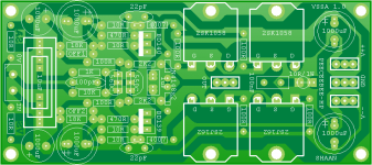
Almost at the end of drawing. Please comment...
Well done Shaan!! PCB looks very nice....
It looks very nice, clean layout with short tracks.Now we have 5mm. Board dimensions: 4.5" x 2.2"

Did you leave out the 470R that was in parallel with the two 1N4148 diodes in your original schematic? I do not see it on the board.
Perhaps it is time to consider a common heatsink for the two drivers, fixed to something else on the board. The higher the supply voltage, the hotter the drivers will run, and the more variance there can be if they happen to heat up unevenly. The heatsink or heatsinks will have to clear the two TO-92 transistors, and also the 10-pm compensation caps on the edge of the board.....I was thinking of how should the heatsinking for the drivers be done properly.
There is also a comment in this thread about attaching a common heatsink to ground...
Thanks all for the comments. Problem areas will be taken care of.
Yes it is best to use single heatsink for vas, simple plate type, or with fins horizontal to the board(the inside of dead atx smps comes to mind, ya i've got two of them in my junkbox") ).
).
I will try to accomodate the VAS heatsink on the board as suggested. Thanks everyone for the tips, also thanks for your patience.
Yes it is best to use single heatsink for vas, simple plate type, or with fins horizontal to the board(the inside of dead atx smps comes to mind, ya i've got two of them in my junkbox
).I will try to accomodate the VAS heatsink on the board as suggested. Thanks everyone for the tips, also thanks for your patience.
I started working on this a few weeks ago, b/c you mentioned it in one of your first posts. There seemed little discussion of the heatsinks in general, so I did not pursue it further.Yes it is best to use single heatsink for vas, simple plate type...
My guess is that assuming the same VAS bias, the temperature of the individual VAS transistors will deviate more with higher supply voltage.
When I made my board layout, I also allowed an anchor-point on the pcb, so that a pin or wire could be attached to the board and help support, and/or ground a common heatsink that did not touch the board, because moving the feedback resistors out of the way was not very convenient.
Attachments
Hi Pete.
Your idea of the anchor point is very good and I will try to implement it in the board. However, I think I'll take some time, some days maybe. It's giving this amateur brain mild nightmares right now and complete re-arrangement is gradually becoming unavoidable(not blaming anybody, I took the task myself).
...I think I'll find a way, haven't reached the limit yet I hope.
I have prepared pdfs of the version with separate heatsink for VAS transistors, it will look like the attachment in post >864<.
If anybody is interested in that version then I can upload the files.
Thanks all for your encouragement.
shaan
Your idea of the anchor point is very good and I will try to implement it in the board. However, I think I'll take some time, some days maybe. It's giving this amateur brain mild nightmares right now
and complete re-arrangement is gradually becoming unavoidable(not blaming anybody, I took the task myself)....I think I'll find a way, haven't reached the limit yet I hope.
I have prepared pdfs of the version with separate heatsink for VAS transistors, it will look like the attachment in post >864<.
If anybody is interested in that version then I can upload the files.
Thanks all for your encouragement.
shaan
First measurements:
I used simple unregulated +/-38,5V PSU. With this voltage total VAS+front end current is over 30mA, almost three times more than it should be. Small VAS heatsinks are very hot. But this is in fact normal since my circuit is made with 16k resisitor. Remedy is to use exactly 35V rails. If you want instant success with parts values on the schematic(s) you must have 35V rails, meaning that you should buy transformer that gives 25V on the secondaries unloadeed, not 25V loaded as I used. Another remedy is to use 18k resitor, or more. My front end BC...Cs are properly matched.
With the relatively small heatsink that I used (Fischer SK92) circuit parameters stabilize relatively quickly (30 minutes).
Biggest surprise is that I could not get DC offset less than 230mV, even with trim pot. I am not sure what is the culprit but I guess its different rank KSA/KSC VAS tranies, that is impossible to match (or unmatched feedback resistors). I used only one 1M trim pot, probably on the wrong side of the circuit. I tested both modules with similar results.
My advice is to follow Shaan's way! Forget about fancy VAS tranies with ultra low Cob. Use cheap and easily available BDs that you can properly match. Use BCs that you can properly match, forget about high hfe rank (C) if you can not find it.
I don't think that can be the only reason, b/c mine are not matched, either (can't match "D" and "E" rank). Only my BC550/560 are matched, and I see in the main VSSA thread that LC does not even recommend that with his module (!).Biggest surprise is that I could not get DC offset less than 230mV, even with trim pot. I am not sure what is the culprit but I guess its different rank KSA/KSC VAS tranies...
Does the offset change at all when you adjust the trim pot, and if it does, by how much? Is it the same on both modules?resistors). I used only one 1M trim pot, probably on the wrong side of the circuit. I tested both modules with similar results.
I don't think that can be the only reason, b/c mine are not matched, either (can't match "D" and "E" rank). Only my BC550/560 are matched, and I see in the main VSSA thread that LC does not even recommend that with his module (!).
Does the offset change at all when you adjust the trim pot, and if it does, by how much? Is it the same on both modules?
During assy I set trim pot to aprox mid position. In that position I have 260mV, and there is some reduction to (230mV) when I turn trim pot very much, probably to end position. I think that for some reason, unknown to me, there should be both trim pots in circuit. But, I can test that only after I dismantle the boards from heatsinks, and that will take some time.
...I used only one 1M trim pot, probably on the wrong side of the circuit.
The solution is to unsolder the trimpot and move it to the other side. This will surely help achieve zero offset. Unmatched feeback resistors have an influence on AC performance but can't affect DC state significantly. It's good to check the 470R at VAS bases. The amp can turn on without these resistors present there, and a defective solder joint can bring hell upon both AC and DC performance of the amp.
Last edited:
Ivanlukic...Biggest surprise is that I could not get DC offset less than 230mV, even with trim pot. I am not sure what is the culprit but I guess its different rank KSA/KSC VAS tranies, that is impossible to match (or unmatched feedback resistors). I used only one 1M trim pot, probably on the wrong side of the circuit. I tested both modules with similar results.
maybe I'm wrong but :
I changed & swapped 2 x 15k resistor to have little DC offset,
+ side 15k & - side 15k seems to work revert if we decrease the value on + side then DC off going to +....
I've measure 15k resistor about 14,86 ohm changed to 14,94 (rail was +/-33VDC)
that little but not that litle
Do you put compensation cap, the value on mine is 33pF
Bias Current and Offset Trim (Long)
@Ivan: I think John may have a good idea, working with the "15K" fixed resistors (or whatever the value is).
The trim pots can be hard to desolder (for me anyway), if they are flush with the board. I have done this a couple times already, and it is easy to ruin the leads of the trim pot.
On the other hand, desoldering and swapping resistors is much easier. So rather than moving the trim pot to the other side, I think I might just work with the fixed resistors.
@John or Shaan, would someone please check my math below, thanks!
My "front end" bias is adjusted to about 18.5mA on both sets of boards I have. This is the sum of the bias at the input transistor, ~2.2-2.5mA, and at the VAS transistor, ~16mA. Calculated from the voltage drop across the 10R which is in series with the diode and the rail voltage.
At this VAS bias current, the case temperature of the VAS transistor is about 18C above room temperature at idle (no audio playing). Measured with thermocouple at the TO-126 case. This may seem a bit high, but the air temperature at the VAS heatsink is already a few degrees above room temperature, due to proximity with the main heatsink. To continue...
1) Input Bias:
Assuming only 15K resistor, one diode drop from the rail to the 15K, and about 0.8V at the junction with the 2200uF cap and the feedback resistor, the untrimmed bias current at the input pair would be something like this:
(VDCsupply - 0.8V - 0.7V)/15K
so in Ivan's case,
(38.5 - 0.8 - 0.7)/15K ~ 2.47 mA
This should be about correct input transistor bias before trimming, and it should be possible to adjust the offset to zero from this point.
The high VAS bias current is a separate issue.
2) High VAS Bias:
Without CCS, the VAS bias current rises disproportionately with supply voltage change. A 5% change in supply rail voltage results in a 20-25% change in VAS bias current. (tested). I am not trying to change the rules of this thread, you can see my post, and reply by Sonnya (including more math), here:
VAS Bias v. Supply Voltage
So if Ivan's supply voltage is about 10% higher than mine, it is quite possible that his VAS bias current will be 10-12 mA higher, which would be close to the 30mA he measured. 30mA unadjusted is within predicted range. So this would not automatically be an error, but it WILL result in a very warm VAS.
(Please correct me if I made any math errors, would not be the first time)
@Shaan: Assuming higher supply voltage and higher VAS power dissipation in the dual mosfet version posted above, this issue will come back, in spades... which brings me full circle to the VAS heatsink discussions... (OK, maybe I just have a one-track mind,)
@Ivan: I think John may have a good idea, working with the "15K" fixed resistors (or whatever the value is).
The trim pots can be hard to desolder (for me anyway), if they are flush with the board. I have done this a couple times already, and it is easy to ruin the leads of the trim pot.
On the other hand, desoldering and swapping resistors is much easier. So rather than moving the trim pot to the other side, I think I might just work with the fixed resistors.
@John or Shaan, would someone please check my math below, thanks!
My "front end" bias is adjusted to about 18.5mA on both sets of boards I have. This is the sum of the bias at the input transistor, ~2.2-2.5mA, and at the VAS transistor, ~16mA. Calculated from the voltage drop across the 10R which is in series with the diode and the rail voltage.
At this VAS bias current, the case temperature of the VAS transistor is about 18C above room temperature at idle (no audio playing). Measured with thermocouple at the TO-126 case. This may seem a bit high, but the air temperature at the VAS heatsink is already a few degrees above room temperature, due to proximity with the main heatsink. To continue...
1) Input Bias:
Assuming only 15K resistor, one diode drop from the rail to the 15K, and about 0.8V at the junction with the 2200uF cap and the feedback resistor, the untrimmed bias current at the input pair would be something like this:
(VDCsupply - 0.8V - 0.7V)/15K
so in Ivan's case,
(38.5 - 0.8 - 0.7)/15K ~ 2.47 mA
This should be about correct input transistor bias before trimming, and it should be possible to adjust the offset to zero from this point.
The high VAS bias current is a separate issue.
2) High VAS Bias:
Without CCS, the VAS bias current rises disproportionately with supply voltage change. A 5% change in supply rail voltage results in a 20-25% change in VAS bias current. (tested). I am not trying to change the rules of this thread, you can see my post, and reply by Sonnya (including more math), here:
VAS Bias v. Supply Voltage
So if Ivan's supply voltage is about 10% higher than mine, it is quite possible that his VAS bias current will be 10-12 mA higher, which would be close to the 30mA he measured. 30mA unadjusted is within predicted range. So this would not automatically be an error, but it WILL result in a very warm VAS.
(Please correct me if I made any math errors, would not be the first time)
@Shaan: Assuming higher supply voltage and higher VAS power dissipation in the dual mosfet version posted above, this issue will come back, in spades... which brings me full circle to the VAS heatsink discussions... (OK, maybe I just have a one-track mind,
)- Home
- Amplifiers
- Solid State
- PeeCeeBee