Indeed, offset is adjusted by turning both trim pots in the same direction, but both must be in circuit. I can not say why both are necessary, but they are. It seems that with symmetrical circuit both halves of circuit ought to be the same.
Hi ivan.
I found that when the input pair is matched then equal value current injection resistors give offset less than 20mV, regardless of high or low hFE and supply voltage(within safe range). And found that it's very easy to bias and offset-trim the amplifier withtout a pot.
First we need to install a fixed resistor on each side to get our desired VAS bias and the E24 standard has enough values for safely doing that (the resistors' values are roughly linearly proportional to PS voltage). Then connect the mV meter to output and connect a fixed resistor between 100k and 1M (say, 470K) in parallel with either of the current injectors and notice which side brings the offset close to zero. That's it and solder the resistor to that side. The offset won't change much as the amp warms up.
shaan
Hi ivan.
I found that when the input pair is matched then equal value current injection resistors give offset less than 20mV, regardless of high or low hFE and supply voltage(within safe range). And found that it's very easy to bias and offset-trim the amplifier withtout a pot.
My input pair was matched to within 20 (610/630), as LC recommends. If I knew that offset be that low I would not install pots at all. I am satisfied with 20-30mV value, that much can not hurt any loudspeaker.
If you want to do it, you can use this for your starting point.
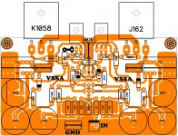
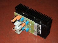
I drew this peeceebee before you made changes. I strictly followed schematic from post #1, just added one more pair of output transistors and source resistors. Size of peeceebee is 140 x 38 mm (5.5" x 1.5").
This is excellent option but, as PMI commented, for this mounting method we would need plated holes for output and VAS tranies, so that all these transistors can be screwed to the heatsink with pins bended, pcb mounted over, and then soldered from components side. Otherwise, it would be very difficult to have all transistors flat on the heatsink surface. And plated holes are not an option for all builders, only for those that can provide pcb factory services.
The unmatched hfe in the VAS transistors should not change the offset, or only a tiny bit. It will have more influence on distortion, through its effect on the positive and negative halves of the signal. We are all in the same boat in that respect. The "E" and "D" parts cannot be matched, and no version of BD139/140 has specs to impress.
In any case, matching the input pair seems more important, and easier to accomplish.
I've bought 10 pcs A1381-E the hFE is 154-156 (quite matched)
then only bought 6 pcs C3503-D the hFE is 78-79 (again quite matched)
but they have a half different of hFE (not good maybe) ...
And I have bought earlier 4 pcs C3503-F hFE is 186-195 & I guess it is better to use

but these C3503-F is non isolated tab (maybe it is 2SC3503-F)
These are the best candidate to use with +/-45V rails, any thought?
note: I bought it from friend live in Tangerang-Jakarta & I believe he bought it from digikey
Last edited:
@John: I think these combinations will work, but I am not sure how well. I also think we are departing from the original idea of using the VSSA circuit in its simplest form, and lowest cost.These are the best candidate to use with +/-45V rails, any thought?
I am a bit concerned that we may be posting something that will be confusing to other people who want to build boards from Shaan's schematic. To the best of my ability to listen, and to measure, the amp sounds very good, and quite tolerant of VAS transistor selection with small heatsinks, up to 35-37V DC rail voltage.
Having said that, as the DC rail voltage increases, and power dissipation increases... :
You are finding the same thing as the rest of us... a truly complementary pair of transistors, with similar hfe, and good (published) specs is hard to find. I think LC used the "E" rank pair for a good reasons.
Personally, I don't think I would use an isolated/non-isolated pair with 45V rails, they will heat up un-evenly, and you can't be certain that they will reach the same temperature. At 45V, and everything else the same, the temperature of the VAS transistor may almost double (voltage and bias current both increase).
A similar thing can be said about pairs with different Cob, D and E pairs with different hfe, and so on. It is hard to say when the resulting distortion will reach a level that you can hear, but sooner or later, it will happen.
(I've done it before, make enough changes from an original concept, and taken in combination, the sound you liked at lower power levels is gone...
)Thanks for remind me, that's why I want to make a new board (2 pairs OP maybe)Now what I'm thinking is make a new Peeceebee that can safely operate at +/-45VDC or more
Yes it's true...(I've done it before, make enough changes from an original concept, and taken in combination, the sound you liked at lower power levels is gone...

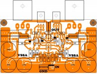
for Shaan, please in check if this is correct?
Hi daman.
Nice drawing!
My thoughts:
1. Double the width of FET source and drain traces.
2. Move the 10R VAS degenerators and compensation caps close to the VAS transistors.
3. Add parallel resistors with 15K current sources(those 'off 1' and 'off 2' marked resistors) for easy offset trimming.
That's all.
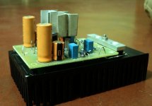
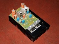
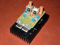
VSSA Power Supply
As posted above, I am working on a capacitance multiplier power supply for my version of PeeCeeBee. A couple of you have expressed some interest in the boards, and/or in etching your own which I heartily encourage... (even though it is not one of my personal talents...) Finished boards will be supplied @ my cost plus shipping, $10 each or very close to that.
(Failing that, I plan to post pics of smoke, rising from my bench, for amusement and edification, chuckle)
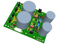
3D renderings of the board are below, pics of the boards to follow in 1-2 days.
(This board is 2-layer, but a single-layer version can be posted to etch your own if desired as soon as I am finished testing)
The circuit design is courtesy of MrEvil, and documented in a separate thread. Like most things I work on, I have tweaked his original layout a bit, but credit for the circuit design should go to him.
http://www.diyaudio.com/forums/power-supplies/53359-finished-capacitance-multiplier.html
http://www.diyaudio.com/forums/power-supplies/51817-improving-capacitance-multiplier.html
I selected this circuit for low cost, and low dropout voltage. With a bit of care, this should give an output which is as clean as the SMPS recommended by LC for the VSSA modules in his GB, at a cost of about 20-25 Euro incl. the board. (less if you have access to some inexpensive caps).
My intention is to post some pics and test results w. PeeCeeBee and VSSA here, beyond that, I plan to keep discussion in the other thread, to avoid making this one even harder to follow...
As posted above, I am working on a capacitance multiplier power supply for my version of PeeCeeBee. A couple of you have expressed some interest in the boards, and/or in etching your own which I heartily encourage... (even though it is not one of my personal talents...
) Finished boards will be supplied @ my cost plus shipping, $10 each or very close to that.(Failing that, I plan to post pics of smoke, rising from my bench, for amusement and edification, chuckle)
3D renderings of the board are below, pics of the boards to follow in 1-2 days.
(This board is 2-layer, but a single-layer version can be posted to etch your own if desired as soon as I am finished testing)
The circuit design is courtesy of MrEvil, and documented in a separate thread. Like most things I work on, I have tweaked his original layout a bit, but credit for the circuit design should go to him.
http://www.diyaudio.com/forums/power-supplies/53359-finished-capacitance-multiplier.html
http://www.diyaudio.com/forums/power-supplies/51817-improving-capacitance-multiplier.html
I selected this circuit for low cost, and low dropout voltage. With a bit of care, this should give an output which is as clean as the SMPS recommended by LC for the VSSA modules in his GB, at a cost of about 20-25 Euro incl. the board. (less if you have access to some inexpensive caps).
My intention is to post some pics and test results w. PeeCeeBee and VSSA here, beyond that, I plan to keep discussion in the other thread, to avoid making this one even harder to follow...
Attachments
Last edited:
My intention is to post some pics and test results w. PeeCeeBee and VSSA here
Please do.
...beyond that, I plan to keep discussion in the other thread, to avoid making this one even harder to follow...
Thank you.

Hi daman.
Nice drawing!
My thoughts:
1. Double the width of FET source and drain traces.
2. Move the 10R VAS degenerators and compensation caps close to the VAS transistors.
3. Add parallel resistors with 15K current sources(those 'off 1' and 'off 2' marked resistors) for easy offset trimming.
That's all.
if this is correct???
Attachments
As posted above, I am working on a capacitance multiplier power supply for my version of PeeCeeBee. A couple of you have expressed some interest in the boards, and/or in etching your own which I heartily encourage... (even though it is not one of my personal talents...
(Failing that, I plan to post pics of smoke, rising from my bench, for amusement and edification, chuckle)
3D renderings of the board are below, pics of the boards to follow in 1-2 days.
(This board is 2-layer, but a single-layer version can be posted to etch your own if desired as soon as I am finished testing)
The circuit design is courtesy of MrEvil, and documented in a separate thread. Like most things I work on, I have tweaked his original layout a bit, but credit for the circuit design should go to him.
http://www.diyaudio.com/forums/power-supplies/53359-finished-capacitance-multiplier.html
http://www.diyaudio.com/forums/power-supplies/51817-improving-capacitance-multiplier.html
I selected this circuit for low cost, and low dropout voltage. With a bit of care, this should give an output which is as clean as the SMPS recommended by LC for the VSSA modules in his GB, at a cost of about 20-25 Euro incl. the board. (less if you have access to some inexpensive caps).
My intention is to post some pics and test results w. PeeCeeBee and VSSA here, beyond that, I plan to keep discussion in the other thread, to avoid making this one even harder to follow...
PMI,
Your design could be easy swap in single layer by changing faston spad place et rooting lane from diode to caps to fuse legs and to caps,no??
Marc
Last edited:
Yes, more-or-less, and thanks for the input.PMI,
Your design could be easy swap in single layer by changing faston spad place et rooting lane from diode to caps under fuse, no??
Marc
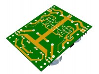
The fastons are on the edge of the board for a good reason (to me anyway). The set of fastons which is near the fuse can be used as an unregulated output - or, input (if the board is used only as a secondary filter). This is realistic for someone who already has a supply for PeeCeeBee assembled, and just wants a cheap and simple alternative to adding more capacitors.
Also routing the trace from the rectifier diodes around the edge of the board increases the HF noise radiated from the rectifier switch-off. This is not so trivial as it seems, because VSSA has a very wide bandwidth, and I can see some of this noise at the output of the amp on my scope. So the wire from the transformer secondary to the rectifier diode, and also the trace from the rectifier diode to the reservoir cap, should both be very short, I think.
I have a slightly different single-sided placement for anyone to etch their own, but I would prefer to wait until I test the circuit. In case there is an error, I would like to find it before someone etched the board and soldered parts...
Perhaps you can give me your input in the other thread, because I do not want to make this one more complicated. This is why I posted the layout there, and not here.
Yes, more-or-less, and thanks for the input.
The fastons are on the edge of the board for a good reason (to me anyway). The set of fastons which is near the fuse can be used as an unregulated output - or, input (if the board is used only as a secondary filter). This is realistic for someone who already has a supply for PeeCeeBee assembled, and just wants a cheap and simple alternative to adding more capacitors.
Also routing the trace from the rectifier diodes around the edge of the board increases the HF noise radiated from the rectifier switch-off. This is not so trivial as it seems, because VSSA has a very wide bandwidth, and I can see some of this noise at the output of the amp on my scope. So the wire from the transformer secondary to the rectifier diode, and also the trace from the rectifier diode to the reservoir cap, should both be very short, I think.
I have a slightly different single-sided placement for anyone to etch their own, but I would prefer to wait until I test the circuit. In case there is an error, I would like to find it before someone etched the board and soldered parts...
Perhaps you can give me your input in the other thread, because I do not want to make this one more complicated. This is why I posted the layout there, and not here.
If you have the have a layout that i can etch my self after you validate work, i am for. In witch thread you will post : the first one or the second (improvement i guess...) that i could subscribe?
Marc
Yes, of course,If you have the have a layout that i can etch my self after you validate work, i am for. In witch thread you will post : the first one or the second (improvement i guess...) that i could subscribe?
Marc
It is here:
http://www.diyaudio.com/forums/powe...hed-capacitance-multiplier-2.html#post3557054


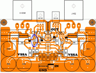
How does this look???
Marvelous Shaan! another professional work from the master. Super
!- Home
- Amplifiers
- Solid State
- PeeCeeBee