Personally I would take a completely different approach and either hold signal lines at gnd (at the input to the amp section) with a delay at switch on and immediately at power off or use a standard speaker protection delay relay. I'd definately no be controlling the mains voltage with a relay (although it would be safe to do so with a correctly rated relay)
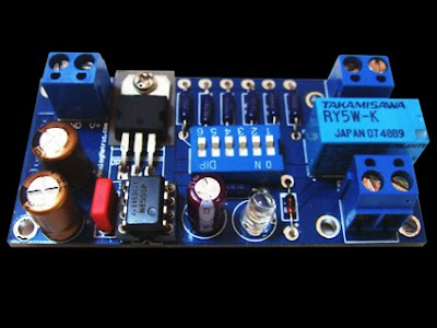
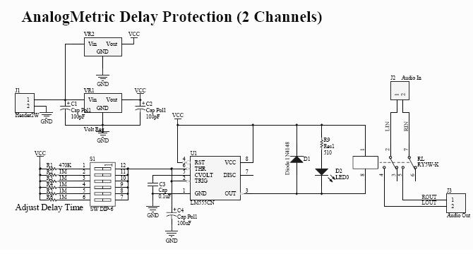
Take a look at this, it may be of some use (bare pcb is also available)
Output Delay Protection DIY Kit (Relay & Adj Timer) 2ch | eBay
Take a look at this, it may be of some use (bare pcb is also available)
Output Delay Protection DIY Kit (Relay & Adj Timer) 2ch | eBay
I completely disagree.I'd definately no be controlling the mains voltage with a relay (although it would be safe to do so with a correctly rated relay)
Many domestic appliances use switches/contacts to control mains voltage. Almost all commercial equipment use only relays to control mains.
I can't understand why you are saying no to relays.
I completely disagree.
Many domestic appliances use switches/contacts to control mains voltage. Almost all commercial equipment use only relays to control mains.
I can't understand why you are saying no to relays.
If you read my post, I didn't say you cant switch mains with relays it or that its not done in commercial application. What I did suggest is that its possibly easier and safer to be messing with a simple signal switch to gnd or output speaker control rather than mains. Admittedly I wasnt specific in my absolute reference to useage but I made the assumption we were looking to deal with this specific issue and not discuss the general use of relays to control mains voltage.....
The problem here is most likely caused by PSU's discharging within the amp therefore playing with the mains input is a backwards way of dealing with the problem. If you pull the mains, you want the output muted immediatlely. A speaker output relay would suffice here if the power down noise comes from the amp section. A delay on start up would also resolve this issue.
If its the DSP thats causing the whining and bumping on power down, the issue can be dealt with by either adding the suggested delay switch in line with the output or by connecting the output to GND immediately after the DC blocking cap when the mute condition is required.
Finally, I'm not aware of any commercial amplifier that uses mains switching as a method control output muting during power up or power down. I'm not arguing with the function of the proposed circuit, but I am questioning if it is the best way to deal with the overall issue???
The original Signetics NE555 had a well known issue inherent in its design of "spiking" the supply as the output changed state. I think a value of 400ma for a few microseconds was somewhere near the mark. That could cause false triggering and erratic behaviour. The recommended solution was a cap as close as possible to the supply pins... and I have just looked at some old data sheets and some mention it and some don't. Some suggest a 0.1 in parallel with a 1uf.
We forget how old these devices are at 40 years 🙂 and there have been many subtle changes and revisions. Later versions and the low power and CMOS versions pretty much eliminated the problem.
Page 8 on this one, additional information
http://www.datasheetcatalog.org/datasheet/nationalsemiconductor/DS007851.PDF
Yes, I was thinking that you were referring to the current spike of the original 555, but I was also thinking that the 0.1 uF capacitor wouldn't store nearly enough charge to smooth out the spike. But then if the spike is for a very short period of time, I guess so.
-Pete
Actually today I did some testing that I should have done originally. See the attachment to my post #35. Omitting my "rapid discharge loop" or resistor R3 and diode D2, and increasing the capacitance of the timing capacitor C1 by ten times, it is impossible to manually disconnect and reconnect power to the circuit quickly enough that output pin 3 of the 555 timer doesn't drop to ground potential. That is, the delay circuit recycles even when there is only a very brief interruption of the supply voltage.
It would seem that the 555 timer provides a low resistance discharge loop for the timing capacitor C1 when there is even only a very brief interruption of supplying voltage to the IC. Is this correct, anybody, do you think, or is there a better explanation?
-Pete
It would seem that the 555 timer provides a low resistance discharge loop for the timing capacitor C1 when there is even only a very brief interruption of supplying voltage to the IC. Is this correct, anybody, do you think, or is there a better explanation?
-Pete
I think it's more by accident than design tbh
Pins 2 and 6 the threshold and trigger pins are inputs to the 555. The discharge pin, pin 7 isn't used. And that anyway discharges to ground via an NPN transistor internally.
I suspect that as power is instantly removed (and there is no decouping cap to maintain power even for an instant) that the timing cap just discharges back into various junctions internally.
Try it with a CMOS TLC555.
That is what I think is happening. It works by exploiting a characteristic of the bjt type 555.
I think it's more by accident than design tbh
Pins 2 and 6 the threshold and trigger pins are inputs to the 555. The discharge pin, pin 7 isn't used. And that anyway discharges to ground via an NPN transistor internally.
I suspect that as power is instantly removed (and there is no decouping cap to maintain power even for an instant) that the timing cap just discharges back into various junctions internally.
Try it with a CMOS TLC555.
That is what I think is happening. It works by exploiting a characteristic of the bjt type 555.
The circuit that I have been testing included a timer IC configured with bipolar junction transistors, NE555. When I changed that timer for a timer using FETs, TS555, I got the same results. That is, both types of 555 timers very rapidly discharge the timing capacitor when the supply voltage is disconnected from pin 8 of the IC.
-Pete
555 will work but is not the right ic for the job. U have to use CD4541 for the purpose and use small value cap as the supply bypass, so that a small interval break in power will also lead to power on reset, which is a feature in this ic.
Gajanan Phadte
Gajanan Phadte
The circuit that I have been testing included a timer IC configured with bipolar junction transistors, NE555. When I changed that timer for a timer using FETs, TS555, I got the same results. That is, both types of 555 timers very rapidly discharge the timing capacitor when the supply voltage is disconnected from pin 8 of the IC.
-Pete
I've though some more about this.
Lets look at the circuit and try and understand what happens. I'm taking it at face value which means that the switch removes power from the IC "instantly". There is no PSU reservoir cap in your diagram which means that the supply collapses instantly. There are only two sources of stored energy, C1 and C2. C2 can be discounted on account of it's value.
That leaves C1.
How is that cap discharged instantly ? If it were under control of the IC then the IC would need to powered and it isn't...
So to see what really happens we replace C1 by a voltage source (and of limited current ability to avoid zapping the IC) and remove the main power.
We find that the IC draws current from this new source (which would be C1 in use) and in this condition the voltage on pins 2 and 6 measure around -0.8 volts with respect to pin 1.
Is the -0.8 volts significant ? Well it points to a parasitic diode formed within the substrate of the IC. That would explain why the CMOS version behaves the same as well. Parasitic diodes that become apparent in these situations are common... many data sheets for all types of IC (opamps/CPU's/logic etc etc often mention that no pin must go more negative than the normal negative pin of the IC because there is a parasitic diode present. If the current is large it can be destructive.
Is it OK to make use of this ? In this case probably, as long as the energy in C1 is small. Is it good design if it uses an "unwanted" characteristic of an IC... that's for you to decide.
Remember, the key feature here is that your circuit instantly removes the supply. If the supply collapses slowly as on an amp for example then the circuit may not behave as expected.
555 timer is perfect for delayed ON and instant OFF.
If care in the design it is OK.
555 will work but is not the right ic for the job. U have to use CD4541 for the purpose and use small value cap as the supply bypass, so that a small interval break in power will also lead to power on reset, which is a feature in this ic.
Gajanan Phadte
Hey, thanks for pointing us to the CD4541. I've looked at the National Semiconductor data sheets for this IC. The way that it functions is a bit more complicated than the 555, but it looks like it would be more useful than the 555 in many applications.
Regards,
Pete
In fact it is much simpler. Some, who do not know the hardware basics will find it bit difficult as 555 is the famous beginner project ic and has more written about than (I think) any other ic.
All u have to do is ground pins 5 and 6 and select pin 8 so that the output stays off in the beginning. Put two 10K pull up resistors at pin 12 and 13(other end to Vdd) Connect 100k to pin 3 and some appropriate value R and C at pins 1 and 2. Pin 10 to Gnd.
Changing the condition at pins 12 and 13, the division can be changed and will change the timing.
In fact knowing this much is more than enough to use CD4541.
N.B. I wrote this from memory.
Gajanan Phadte
Last edited:
So to see what really happens we replace C1 by a voltage source (and of limited current ability to avoid zapping the IC) and remove the main power.
We find that the IC draws current from this new source (which would be C1 in use) and in this condition the voltage on pins 2 and 6 measure around -0.8 volts with respect to pin 1.
Is the -0.8 volts significant ? Well it points to a parasitic diode formed within the substrate of the IC. That would explain why the CMOS version behaves the same as well. Parasitic diodes that become apparent in these situations are common... many data sheets for all types of IC (opamps/CPU's/logic etc etc often mention that no pin must go more negative than the normal negative pin of the IC because there is a parasitic diode present. If the current is large it can be destructive.
It beats me how it is possible to end up with a voltage below ground at pins 2 & 6 and how a parasitic diode could effect this. I'm not disputing the -0.8V, I've measured a negative voltage at pins 2 & 6 myself. But certainly somehow the "dead" timer IC is providing a discharging loop for the timing capacitor.
Before connecting V+ to the delayed power-on circuit, try disconnecting pin 1 of the 555 timer from ground and see if the timing capacitor will take a charge.
Regards,
Pete
It beats me how it is possible to end up with a voltage below ground at pins 2 & 6 and how a parasitic diode could effect this.
Juggle the circuit around. I tried to think of a way to make it easy to explain 🙂
When powered normally we measure 12 volts on pin 8 and zero volts on pins 2 and 6. The timing cap has charged normally and has 12 volts across it.
When we remove the supply the positive, the positive end of the cap (which is also pin 8) will have a conductive path via the chip to pin 1. (Just imaginge the chip as a 10k or a 100k or a 1meg even between pins 1 and 8).
Our meter negative lead although it hasn't moved off pin 1 is also now "connected" to pin 8 via this internal resistor (the circuitry of the 555). If we measure on pin 2 and 6 we see a negative voltage. That's because the negative end of the cap is at -12 volts relative to the positive end.
If there were no diode action or leakage it would read -12 volts. That we read -0.8 is due to the clamping action of an internal diode.
Plenty of ways to skin this cat.
Here's one which counts mains cycles for the delay.
(This image is just 76k, so will insert it inline below.)
Caution - as drawn, it is directly powered off the mains, but it should be
simple to power it off a lower voltage tap (6.3V ac, for eg).
Geek pointed out on another forum that the timing chart is based on 50Hz.
For 60Hz, the timing increments will be in 4.25 seconds instead of 5.1
An externally hosted image should be here but it was not working when we last tested it.
Remember me🙂
Well even though I have had the parts for 2 years I never got to built the boards🙂
I am trying to tidy up lots of loose ends with the projects and this is one of them. I have learnt a little bit about Eagle and had a couple of very simple boards made. I was hoping you would do me another favour & check the schematic & PCB I have drawn to see if Iv'e missed anything obvious before I get them made. It's a bit messy because I was trying to cram it into a small space. You'll have to excuss the relay symbol, I know it's not the way there normally shown but I drew it so I would understand it. also the PCB is not showing the ground connections but they are there, whatevers not connected to a wire is connected to the ground plane.
I have attached the agreed design from 2012, the new schematic & the PCB layout.
Attachments


- Status
- Not open for further replies.
- Home
- Amplifiers
- Solid State
- Delay On/Off Setup