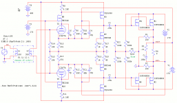
Was playing around in SPICE combining some different ideas and came up with this hybrid. Output is circlotron and I'm aiming to play around with those SemiSouth SJEP120R100A silicon carbide static induction transistors (modern power jFET). The INXS mos as shown is just a placeholder.
Bias feed will need some more stability, and a required power on delay relay, etc.. but I think the topology looks usable for the high powered bass amp I'm going for.
Anyone have any thoughts on this before I breadboard it?
Bias feed will need some more stability, and a required power on delay relay, etc.. but I think the topology looks usable for the high powered bass amp I'm going for.
Anyone have any thoughts on this before I breadboard it?
Attachments
")
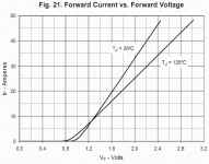
A real static induction transistor would have voltage amplification
factor "Mu", and the curveset of a triode. This one looks a really
big enhancement mode JFET to me. With much as 1A of gate to
source forward bias current. You will never drive that sort of A2
with 100K "gate leak" bias...
Maybe you linked us the wrong specsheet?
factor "Mu", and the curveset of a triode. This one looks a really
big enhancement mode JFET to me. With much as 1A of gate to
source forward bias current. You will never drive that sort of A2
with 100K "gate leak" bias...
Maybe you linked us the wrong specsheet?
Also note reverse transfer (Miller) capacitance varies from 60pF to 600pF
over the 170V-10V range of drain voltage I expect you are shooting for...
In a lot of ways, this part is far harder to drive than its worth. Its not
voltage linear (not a SIT) , nor is it current linear, nor is its capacitance
stable, demands gobs of forward gate current (worse than 2n3055).
What was the point again?
You need to forget SIC enhancement JFET and look you to IGBTs.
Last edited:
IXYS SEMICONDUCTOR|IXGH48N60B3C1|GenX3 SILICON CARBIDE (SiC) IGBT | Newark.com
At least Miller capacitance stays below 100pF down to about 13V... And no forward gate current.
Why you not using quadrature feedback to shape output currents and prevent thermal runaway?
You probably need serious current control anyway, just to keep from redlining wires in your wall.
At least Miller capacitance stays below 100pF down to about 13V... And no forward gate current.
Why you not using quadrature feedback to shape output currents and prevent thermal runaway?
You probably need serious current control anyway, just to keep from redlining wires in your wall.
Last edited:
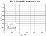
I guess it could work if you could keep the case at 25C. You will probably have to use refrigeration or more parts to get that much power. Use full face shield.
Haha.. I only expect 9A per device. Even at 150C, that's off the chart for figure #5 and below 1mA
Ick. Thanks though.
At least Miller capacitance stays below 100pF down to about 13V... And no forward gate current.
Why you not using quadrature feedback to shape output currents and prevent thermal runaway?
You probably need serious current control anyway, just to keep from redlining wires in your wall.
I'll get there... The part has a negative thermal behavior. See Fig #1 vs #2. I don't think degens will be needed.
IGBTs? Those are probably the worst parts to ever be used in linear amplifier applications. They are commonly found for high voltage pulsed applications like power inverters. IGBTs go thermal rather easy from my experience
SIC ain't your grandma's IGBT.
Maximum are 300W, 150C, 75A.
Attachments
SIC ain't your grandma's IGBT.
Maximum are 300W, 150C, 75A.
Compare Fig#1 to Fig#3 and see that it suffers a positive thermal behavior. Not something I consider beneficial in an audio output stage.
Compare Fig#1 to Fig#3 and see that it suffers a positive thermal behavior. Not something I consider beneficial in an audio output stage.
No idea why you would let an output device decide its own current anyway.
Its not like choosing such a part has made your design "simple". Ain't gonna
help if you driver transistor now runs away trying to feed this black hole of
a JFET gate from Hell...
Attachments
Last edited:
Your observation Fig 1 and 3 are correct, but your conclusion incomplete.
Below 7.5A, yeah you gotta do something to keep a quiescent in check.
Above 7.5A, tempco is safe. Runaway beyond 7.5A not gonna happen.
I'm not saying this fact alone gets IGBT out of the fire...
I suggest again quadrature feedback. Currents are then totally slave to the
sensible rule of as few as three cold devices. Why work so hard to control
the output voltage, but let final stage current to chance and temperature?
Last edited:
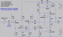
Currents can't run away when you use a feedback loop to shape them.
I show you the simplest 3 parts class A. But class AB can be shaped
almost as easily, replace sense resistors R11+R12 with cold Schottky
diodes. Q4 would be on same hot sink with the outputs, diodes not...
This topology (at higher voltage) would not be a bad starter for your
SIC JFETs. The challenge to steer big drive current is similar.
Attachments
Last edited:
- Status
- This old topic is closed. If you want to reopen this topic, contact a moderator using the "Report Post" button.
- Home
- Amplifiers
- Solid State
- 1.4kW; is this crazy?