Hi Mir,
I'm not sure if I understand you correctly. But I'm afraid you are missing one important point: The whole thing (regarding AB-II as well as Class-I) is based on nonlinear FB as far as the bias loop is concerned. This scheme approaches the so called geometric mean relationship between the currents through the top and bottom OP devices, i.e Idp * Idn = constant. To keep the product of these current exactly constant is not an aim in itself (any relationship will do), rather the aim is to prevent that one of the two OP devices gets completely turned off. If this might happen the, relationship between the two currents is undefined by definition.
Going back to your suggestion (if I understand you correctly), if you linearize the bias FB loop, then, above a certain output current, one of the OP devices will be completely turned off. That's exactly what we don't want.
BTW, I've simulated such approaches, but to no avail; much more distortion.
Cheers,
E.
PS: As for schematic capture, why don't download the student version of Micr0Cap V10. It's for free and the easiest and fastest SW you can get.
Hi Edmond,
I case if used more then one pair of output transistors what is better to connect, only one pair to error feedback and auto bias transistors, or do it from each pair? In my schematic resistors are R58, R60, R59 and R61.
Damir
I case if used more then one pair of output transistors what is better to connect, only one pair to error feedback and auto bias transistors, or do it from each pair? In my schematic resistors are R58, R60, R59 and R61.
Damir
Attachments
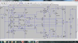
'doubled transistors'
Hi MT
No, it are the resistors R47, R55, R54 & R56 that reduce the tempco.
Regarding the 'doubled transistors', see: http://www.diyaudio.com/forums/soli...ogy-construction-troubles-44.html#post2817250
Cheers,
E
Hi MT
No, it are the resistors R47, R55, R54 & R56 that reduce the tempco.
Regarding the 'doubled transistors', see: http://www.diyaudio.com/forums/soli...ogy-construction-troubles-44.html#post2817250
Cheers,
E
Hi Damir,
You are referring to the so called Barny Oliver optimum point, i.e. 26mV across both emitter resistors. In case of AB2 your are simply bound to this 33mV (across a single resistor). I am not sure whether this is a real disadvantage or not. I have to figure that out.
Cheers,
E.
You are referring to the so called Barny Oliver optimum point, i.e. 26mV across both emitter resistors. In case of AB2 your are simply bound to this 33mV (across a single resistor). I am not sure whether this is a real disadvantage or not. I have to figure that out.
Cheers,
E.
Barny Oliver
Hi Damir,
Indeed, some gm doubling takes place. So I simmed the OPS with 26mV across both emitter resistors, being the optimum bias (by means of two multipliers, easy to simulate, harder to build). Guess what? Distortion gets worse! Apparently, different rules apply to output stages with a sliding bias. So forget Barny Oliver with all his wisdom.
Cheers,
E.
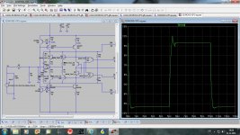
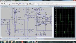
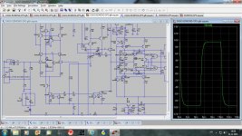
AB2 square wave simulation
Hi Edmond,
I did some simulation with square wave, and it is not very encouraging. If I test with a bit higher input signal it vent berserk.
First test is solo OPS. Slew Rate cca 80V/usec
Second is full amp with no input filter connected.
Third test with input filter connected, Slew Rate cca 30V/usec.
What do you think about it? Not very promising.
Damir
Attachments
Not very promising.
Hi Damir,
I'm not surprised at all, as you are torturing the OPS. For two reasons you got ugly results:
1. Drivers for the top respectively the bottom OP devices consist of only a single EF stage instead of a push-pull stage. Regrettably, it's a bit difficult to implement the latter, as such arrangement will compromise the headroom of the bias circuit. (Therefore, I prefer vertical MOSFETs, with a much higher Vgs than the Vbe of a BJT). Sliding bias schemes are crying for separate push-pull drivers, as a speed-up capacitor (between the emitters) is forbidden. If you still insist to use BJTs, well, it has a prise.
2. Because of the limited speed of the internal loops inside AB2 (the ULGF is 'only' 3MHz) you must filter the transients of a square wave test signal drastically, preferable by means of a 2nd order Butterworth low pass filter with a Fc of around 250kHz. In this way the slew rate, or more precisely the rise and fall time is kept to a safe value. Now, it may look as if the slew rate is limited (to 50V/us or so), but actually, we are dealing here with a finite rise and fall time. Nothing wrong with that as long as it is determined by a filter and not by deficiencies of the amplifier itself.
BTW, in case of a 1st order filter, you have to chose Fc much lower. That's why I recommend a 2nd order filter.
(hope this helps)
Cheers,
E.
Hi Edmond
Once again my poor English leads to possible misunderstanding. It is because the posts to this thread are the first attempts of English language conversation on technical issues for all my life. I’ll make another try some days later.
Cheers Mir
Hi Mir,
No problem and don't give up.
")
Drawing a schematic will also help to avoid confusion. Do you have a scanner? If so, just draw it with pencil and paper.
Cheers,
E.
(...) you must filter the transients of a square wave test signal drastically, preferable by means of a 2nd order Butterworth low pass filter with a Fc of around 250kHz. In this way the slew rate, or more precisely the rise and fall time is kept to a safe value. Now, it may look as if the slew rate is limited (to 50V/us or so), but actually, we are dealing here with a finite rise and fall time. Nothing wrong with that as long as it is determined by a filter and not by deficiencies of the amplifier itself(...)
To avoid the overshooting, I was wondering why "filter the transients of a square wave test signal drastically" is here acceptable, while for a two pole compensated amp it's "a fake solution": http://www.diyaudio.com/forums/soli...lls-power-amplifier-book-129.html#post2418656
Hi Edmond,
Is that what transistor is replaceable with cheaper, I mean is it ok if I replace them with 3904-3906?
Damir VAS is saturated in squarewave test, and it is three stages so it need more time to recover. Ofcourse Audio amp won't eat any square waves, using filter will help.
Is that what transistor is replaceable with cheaper, I mean is it ok if I replace them with 3904-3906?
Damir VAS is saturated in squarewave test, and it is three stages so it need more time to recover. Ofcourse Audio amp won't eat any square waves, using filter will help.
Hi Edmond,
Is that what transistor is replaceable with cheaper, I mean is it ok if I replace them with 3904-3906?
Hi Ontoaba,
Sure, that is, if you take the time and effort to (hand) select them for tight matching of Vbe, within a few mV.
As an aside (and joke), one might argue that, given the time to select the right trannies, AB2 doesn't deserve the name 'auto bias' any longer, as setting the bias by means of a trim pot takes far less time.
Damir VAS is saturated in square wave test, and it is three stages so it need more time to recover. Of course Audio amp won't eat any square waves, using filter will help.
You're right, amps won't eat any square waves. Tortured with infinite fast transients any amp will be pushed beyond its limits.
In case of this amp I don't know yet what causes it to get 'berserk'. Saturation, lack of headroom of the bias circuit, missing Baker clamps? With vert. MOSFETs I got much higher slew rates. Maybe AB2 doesn't like BJT output devices anyhow. I have to figure that out.
Cheers,
E.
(...)amps won't eat any square waves. Tortured with infinite fast transients any amp will be pushed beyond its limits.
As far as I can tell, from both theoretical and practical perspectives, this is incorrect. Both bandwidth and slew rate limitations are not good reasons for any amp to go "beserk", as long as signal levels are beyond clipping.
Care to support your statement?
The reason for the overshooting response of your autobias scheme is to me pretty obvious: the forward and the nonlinear reverse autobias feedback paths have local close coupled poles. And, to add insult to injury, the forward path is also nonlinear, as the forward pole is signal level dependent (being mostly defined by the mosfet Miller capacitance, strongly nonlinear when Vds approaches zero), hence a worsening in the step response at clipping onset.
Unfortunately, although it is possible to separate these poles (the LT1166 circuit mentioned in another thread is a good example, with the loop input filter, per the datasheet application example), but then most of the spectacular distortion reduction effect would be lost. A trade is required here, don't know how far it can be pushed. As it is though, I don't think the current step response is acceptable for audio applications.
push-pull drivers
Hi Damir,
As I explained elsewhere, in order to discharge the gates or bases of the OP devices, you really need separate push-pull drivers, as you can't use the ubiquitous speedup cap. Without them, of course the OPS 'went berserk' when subjected to an unconditioned square wave.
In the meantime I've figured out how to implement such drivers* (without compromising the headroom of the bias circuit). Now, the square wave response is much better. You still need a filter (anyhow), but I could increase the cutoff frequency to 500kHz with out any troubles. Without filter, hardly any overshoot (rather 'undershoot') and more seriously, an enormous cross-conduction. Needless to say to avoid that at any time.
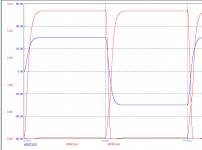
Below the SW response at 50 KHz and 30Vpk. Blue = Vout; Red = Ie; Max. SR = 100V/us. Notice that there is still some cross-conduction: about 1A, though during a very short period of time: less than 1us.
* at the expense of 4 additional trannies, two for the drivers and two for the bias spreaders.
Cheers,
E.
PS: I'm sorry for the interference by Mr Troll. I've put him on my ignore list. Hope it helps.
Hi Edmond,
I did some simulation with square wave, and it is not very encouraging. If I test with a bit higher input signal it vent berserk.
[snip]
Damir
Hi Damir,
As I explained elsewhere, in order to discharge the gates or bases of the OP devices, you really need separate push-pull drivers, as you can't use the ubiquitous speedup cap. Without them, of course the OPS 'went berserk' when subjected to an unconditioned square wave.
In the meantime I've figured out how to implement such drivers* (without compromising the headroom of the bias circuit). Now, the square wave response is much better. You still need a filter (anyhow), but I could increase the cutoff frequency to 500kHz with out any troubles. Without filter, hardly any overshoot (rather 'undershoot') and more seriously, an enormous cross-conduction. Needless to say to avoid that at any time.
Below the SW response at 50 KHz and 30Vpk. Blue = Vout; Red = Ie; Max. SR = 100V/us. Notice that there is still some cross-conduction: about 1A, though during a very short period of time: less than 1us.
* at the expense of 4 additional trannies, two for the drivers and two for the bias spreaders.
Cheers,
E.
PS: I'm sorry for the interference by Mr Troll. I've put him on my ignore list. Hope it helps.
Attachments
- Status
- This old topic is closed. If you want to reopen this topic, contact a moderator using the "Report Post" button.
- Home
- Amplifiers
- Solid State
- Class i and siblings