Hi All,
There is a good article here:
Safe Operating Area calculations
with a triple-slope SOA circuit. You can also DL an XLS calculator to work out the resistor values based on the supply voltage and SOA of the OP transistors
There is a good article here:
Safe Operating Area calculations
with a triple-slope SOA circuit. You can also DL an XLS calculator to work out the resistor values based on the supply voltage and SOA of the OP transistors
Will this protection circuit impair amplifier sound quality?
Of course it will reduce output power the limit should be at 10 amps &110 volts.
FWIW. Your resistor values obtain figures of 2.86 amps and 97.53 volts. (Assuming rails of 55V, Re = 0.22R and Vbe = 0.6V).
Brian.
Refs. Michael Kiwanuka (EW Oct 2002)
Eric Mendenhall. (AES 5695 Oct 2002)
I made a test on a MPS8099 I had a lot in stock, and found 0.68 volts, rails at 55 are close to real values in my amp.
If we scale your numbers according to polarisation voltage, and we assume 3 output transitors, we have perfect match, your simulation confirm my calculation.
I am glad to see this, a confirmation of our work is always welcome.
Tank you.
If we scale your numbers according to polarisation voltage, and we assume 3 output transitors, we have perfect match, your simulation confirm my calculation.
I am glad to see this, a confirmation of our work is always welcome.
Tank you.
cascode polarisation
I just notice this morning that the reference point for the voltage divider ( R18-R19- C6 ) for cascode transistors ( Q3-Q4 ) is on the dirty ground instead of the signal ground.
Is it the best position ??
Will this bring noise in the input section ??
I just notice this morning that the reference point for the voltage divider ( R18-R19- C6 ) for cascode transistors ( Q3-Q4 ) is on the dirty ground instead of the signal ground.
Is it the best position ??
Will this bring noise in the input section ??
I just notice this morning that the reference point for the voltage divider ( R18-R19- C6 ) for cascode transistors ( Q3-Q4 ) is on the dirty ground instead of the signal ground.
Is it the best position ??
Will this bring noise in the input section ??
Not the "dirty" ground ... but a separate "unlifted ground". A very minor
consideration. Each section of the amp has a separate feed from the star
ground. The small signal section even has a separate CRC PS.
Most reviews/impressions tell of total silence.

PS - I did improve this on the wolverine ... removed the cascodes
reference from ground entirely. Some say this improves things ....
maybe a V2.5 ???
You could use the "luxman" method ... and not reference the cascode
from a grounded zener (the jumper for the cascode options).
I left this as a option...
OS
I'll vouch for dead silence using the unlifted ground reference. Sounds great.
OS, are wolverine boards going to be available? As a University of Michigan alumnus, I have to have one.
Wolverine goes with the "slew triple" ... If Jason sells these boards out ,
I will consider donating the wolverine/EF3 design to DIYA (a V2.5).
OS
feedback & phase margin
I tried to calculate and understand bandwith reduction with a capacitor across R6
If I ad a 33pf across R6 it will reduce gain at high frequency.
At 146kHz gain will drop by 3 db ant wiil be 29 instead of 41.
But there will be 43.6 degres of leading phase shift in the feedback circuit.
According ti me this phase shift will be '' insinde loop '' and will increase phase margin and stability.
Is it the case ??
Post 886 and post 888 have some relevant looking discussion.Hi, Apparently thre was some discussion here how to prevent output transistors blowing? What was it? Replacing TMC with Miller? anything else? As this thread has over 120 pages would someone remember roughly relevant page numbers? Thank you, cheers,
Thanks,
My CCS is set to deliver 3.1mA to LTP so VAS gets somewhat lower current and my VAS radiator is 3mm thick and 50% larger. I also have R24=1.2k with C7-8: 81pF and 390pF and BAS45a between Q9 and 10.
audiofan,
It'd be nice to have a current protection circuit included. I wondered why os did not include it as those who don't like it could simply ommit it. Now it's more difficult to incorporate. It would have to be built on a small, separate board and connected to the main one somehow. This is the difficult part. Did you do it? If yes could you show how?
I never used a circuit you have shown. Mine were simple circuits sensing currents at only one N and one P emitter resistors with quality C about 47-68uF to reduce chances for oscillations and giving some 50-70ms peaks "headroom". I never used R accross Vce (to V+ and V-) as I do not know what the optimum bias current to the bases of protection transistors would be.
cheers,
Last edited:
Thanks audiofan,
You might consider adding caps between bases of T1 and T2 and Vout to introduce some delay so for short time higher currents could flow. This cap also reduces chances for oscillations, which are likely to happen when the circuit is activated and deactivated.
What transistor (T3 in your diagram) did you use for VAS protection? I have never done it before.
cheers,
There is 33 nf across base and emitter of protection transistors... I forgot to ad it on the desing ....
The third transistor is a current limiter for Q10 ..... This one will limit current in Q10 to 20mA .... must remember that when output protection get in system is no longer linear .... input will get unbalanced and will push Q10 to saturation or to cutoff
If it goes to cutoff there will be no problem but if it goes to saturation you will have a very high current in Q10 and in the protection transistor.
I still have no clue about adding a capacitor across R6 ....
Adding 33pf will reduce max frequency to 146 kHz and change phase margin ...
Will the amplifier be stable or will it go in oscillation ??
I did ask in post 1228 .... but did have any comment ..
"LC" was added as a "option" ... most have commented that it
does nothing for SQ. Leave it empty.
"Badger" is pretty tolerant of compensation ....
Keep C7/8 close ( 100/470p).
You might want to increase R24 to 1.2-1.5K , member "still4given"
had slight ringing at 820R.
All should be well with these values.
PS - for my subwoofer badger , I'm going to jumper C8 - omit R24.
The advanced "TMC" comp. won't matter at all from 20-100HZ !
Just simple miller 100pF ultrastable bass amplification ....
OS
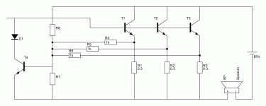
Here is a typical circuit.
R4- R5- R6 set to a ''medium value ''
To set maximun current in transistor
Assume T1-T2-T3 at saturation (no voltage drop across them)
Voltage drop across R8 is zero , current across R8 is zero
If maximun current of each transistor is 4 A ( speaker current will reach 12A )
Voltage across R1-R2-R3 is 1.2 volts
Assume voltage to get T4 conducting is 0.65 volt
Voltage drop across R4-R5-R6 is 0.55 volt ... current is 0.55 mA each ... total current is 1.65 mA through R7...
So R7 should chosen to have a voltage drop of 0.65 volts with a current of 1.65 mA then ...... 394 ohms ( practical value 390 )
Now set maximum voltage at transistor ( with this value of voltage across transistor transistor current will drop to zero .
Assume T1-T2-T3 at cutoff ( zero current through them )
R1 in series with R4 ...... R2 series with R5 ....... R3 series with R6 .... all 3 set in paralell ........ equvalent value 333.4 ohms.
Then in paralell with R7 ( 390 ohms ) equivalent value of 179.7 ohms
To get T4 in conduction ( 0.65 V ) you must have 3.62 mA through 179.7 ohms..... must have 3.62mA through R8
If you want maximum voltage at transistor to be 120 Volts ... R8 should be 33149 ohms ( 33 k ohms )
Attachments
Thanks audiofan,
4A seems to be high for my MG6331/9411 transistors and PS voltages of about +/-63.5V no load. MG6331/9411 at about 65V Vce should survive 4A DC (SOA) but with such currents - although voltage will drop probably to about +/-56V allowing for just below 40V RMS signal - temperature will be over 60C so maybe 2.5A would be more appropriate (SOA derating figure shows P drop from 300W to 200W at 60C) with a cap allowing for 35ms to 50ms delay allowing for higher currents for that period?
What do you think?
What transistors and PS voltages do you use?
cheers,
- Home
- Amplifiers
- Solid State
- diyAB Amp - The "Honey Badger"