Better if you guys plan a group buy , this will reduce costs and enable others who find difficulty in making double sided PTH[plated through hole] boards, to enjoy the amplifier.😉
Copper thickness should be 35micron required minimum on both layers and plating in holes is needed as there are Vias in the PCB which connect both layer tracks at some point.
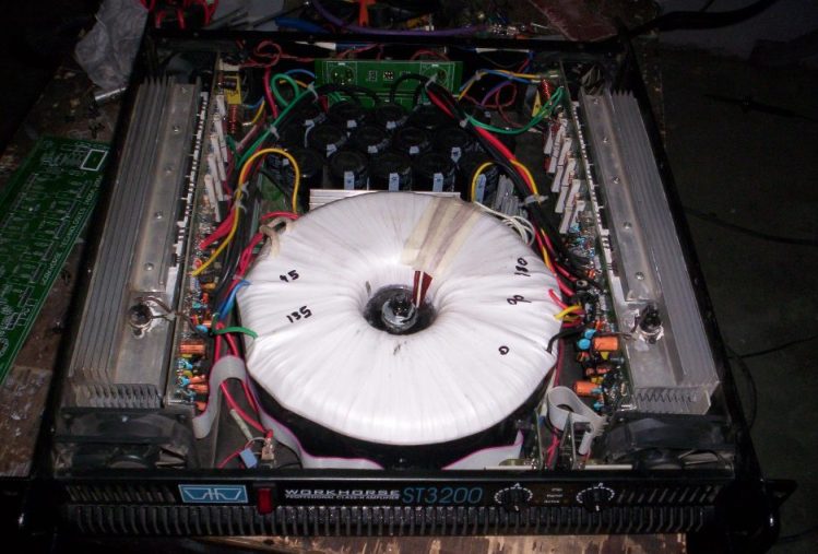
The amp is very easy and required parts are very easy to get.
BC546/556, MPSA42/92, MJE340/350, 2SC5200/SA1943, UF4007, 4N25 OPTO, LM393, NE5532 are some of the main items you need for this, apart from this are usual passive resistors and capacitors.
I will provide construction details after i will see a PCB from anyone of you.😎
Maybe it is better to supply us as kits so we have no problem colecting parts.
Maybe it is better to supply us as kits so we have no problem colecting parts.
Who will pay?
hi workhorse
greetings i am having problem how to open pcb in traxmaster
can you tell me how to open pcb file as i want to make this amp very quickly
any schematic for this amp
thanking you
andrew lebon
greetings i am having problem how to open pcb in traxmaster
can you tell me how to open pcb file as i want to make this amp very quickly
any schematic for this amp
thanking you
andrew lebon
hi workhorse
greetings i am having problem how to open pcb in traxmaster
can you tell me how to open pcb file as i want to make this amp very quickly
any schematic for this amp
thanking you
andrew lebon
Sch is in post 17,
Go to Traxmaker and open the file simply
Sch is in post 17,
Go to Traxmaker and open the file simply
use GrebMagic
😕is this some kind of TRADE SECRET?
Copper thickness should be 35micron required minimum on both layers and plating in holes is needed as there are Vias in the PCB which connect both layer tracks at some point. VIAS IN THE PCB?
can home made pcb meet this?
if pcb vias not met,will the amp still stable?
Copper thickness should be 35micron required minimum on both layers and plating in holes is needed as there are Vias in the PCB which connect both layer tracks at some point. VIAS IN THE PCB?
can home made pcb meet this?
if pcb vias not met,will the amp still stable?
Last edited:

😕is this some kind of TRADE SECRET?
Copper thickness should be 35micron required minimum on both layers and plating in holes is needed as there are Vias in the PCB which connect both layer tracks at some point. VIAS IN THE PCB?
can home made pcb meet this?
if pcb vias not met,will the amp still stable?
There is no Trade secret, This is normal thing in double sided PCB where VIAS are used............to connect one or more layers.
IF Vias are left unconnected, the circuit may not work. This is not you normal single sided pcb.
Last edited:
hope it helps
Jay, in those PDFs TOP and BOTTOM. The PCB boundary marking is touching the traces, don't include the boundary marking while etching the pcb, other wise a short will occur. The boundary layer is either keepout layer or mechanical layer.😀
Last edited:
Jay, in those PDFs TOP and BOTTOM. The PCB boundary marking is touching the traces, don't include the boundary marking while etching the pcb, other wise a short will occur.😀
Ty for the Info,
Pls check
Attachments
Last edited:


Ty for the Info,
Pls check
TOP AND BOTTOM are Perfect now..........But you can keep boundary in TOP OVERLAY
IF PTH is unavailable, one can still make use of dual layer pcb and solder both sides of component pins in order to make the connection work.

- Status
- Not open for further replies.
- Home
- Amplifiers
- Solid State
- "DIY 1.5KW Bipolar Class-H"