Hi Buzz1167
I believe that on your schematic you have connected your DC supply rails labeled Hi & Lo on the wrong side of the 10 ohm rail resistors. If you intend to connect your amplifier this way, these resistors will blow as soon as it was powered up.
Otherwise a very nice job.
Philip
I believe that on your schematic you have connected your DC supply rails labeled Hi & Lo on the wrong side of the 10 ohm rail resistors. If you intend to connect your amplifier this way, these resistors will blow as soon as it was powered up.
Otherwise a very nice job.
Philip
you think like Doc Cherry and I try to adopt.
Dear Andrew,
I have only very few theoretical education or experience but I keep my eyes and ears open.
I adopt different ideas on PCB's. I was blowed away when I started to stack all high current polygons on top of each other on a 4 layer board (V+, V- and output), and rout it from one side. Keep all the low current lines on the other side, and keep loops as short as possible. With the same design I saw the THD dropping significantly to levels I could't even believe I was ever able to archive.
You can say I've seen the light
 . Of course there is never an absolute truth in audio, and every one adopt/prefer own principles. I like the principle of keeping high current planes as close as possible, preferable stacked on multiplayer board.
 With kind regards,
Bas
Thanks Max Caliber, I have messed up one of the transistors, and no I don't plan on powering the thing backwards.
I've also upped my capacitors to 2x220uF 1x4.7uF for the output set and 1x220uF 1x4.7uF for the input set. The 4.7uF's are also low impedance caps because the cost was insignificant. I did this mainly because I didn't like the RC constant of the 100u 10R setup I thought it should be larger for rejecting power transistor noise.
I have also read an article on the electrolytic caps very high frequency operation being mainly inductive and thus the need to stagger the cap sizes down like was suggested here. I haven't experienced this first hand, but then again I might not hear the difference unless extensive testing was done. I thought it an easy addition to add another 5mm cap even if I may not notice the difference.
Andrew and Sebastiaan:
Is there any documentation on the techniques you are referring to? I like the ideas presented but don't have any experience in actually doing it. It sounds like you are both suggesting that the positive and negative rails are generating EM fields across them and thus encompassing the entire small signal section when someone (like myself) chooses to place them at the top and bottom of the circuit.
I should then, by observation of what not to do, choose to place them as close together as possible and run small traces to the required components? Does it not matter if the the ground, output, and +-Rails are all close together? They can apparently not cause enough influence at that level of current to cause issues?
Thanks for your responses so far.
Victory!
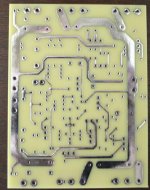
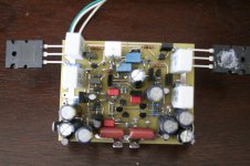
So I figured I would post the results of this little debacle of a design. I have completed testing on my low power setup so I'll be moving up now. I'll admit that working on it after its been built is less than ideal, but its not as bad as I thought it would be based on how much crap there is on there.
Ive had to replace a CCS because I must have burnt it up with the iron somehow, it wouldn't sink current properly which made for some really awkward first tests.
I also have these boards finished or unfinished to sell if anyone's interested cuz I know me and I bought extra in case I screwed some up. I don't have as nice a design as some others on here but I figured I'd throw it out there, I'll probably just toss them on ebay.
I ended up using a 220x100x4.7uf power cap setup and a 10ohm-220x4.7uf for the small signal power as you can see in the corners. Obviously the CCS's are adjustable but I don't think I need to do anything with them right now. I also went with some really awesome radially terminated 0R22 emitter resistors to save space, they are great!
I'd like comments for future designs. I'm working on the power/ground setup to try and get it all in line and to one side for a future design. I'm not sure if I would go partial surface mount or not... Maybe.
Thanks to everyone for the help!
Attachments
- Status
- This old topic is closed. If you want to reopen this topic, contact a moderator using the "Report Post" button.