Hello again crew, I'd like to first thank everyone who's helped me though this learning process so far and I hope that I'll be able to give something back in the near future.
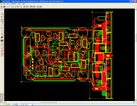
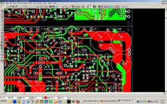
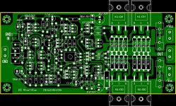
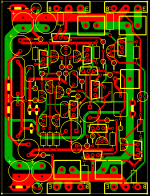
My hopefully final 'generic question' is about PCB layout, I have done my best using the PCB express software utilizing 2 layers and assuming that I will be making boards for their standard service (No silkscreen, No soldermask), So pardon the absence of descriptive silkscreen layers.
I'd like some comments on ways that I've setup things and possible better ways to do them, I have provided the two individual layers as well as the combo with and without the silkscreen. In case you notice, I'll place some components on the back of the board, notably the input caps (2x in parallel because it was cheaper), most of the power caps, and the emitter resistors otherwise they wont all fit and it will be really tight. Maybe someone will find some errors too, I hope so...
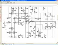
I made some new symbols based on components I have;
1) The circle with the line on one side is a resistor (stood up on end)
2) The squares on the outputs are emitter resistors that are terminated radially (I thought it would save a lot of space)
3) Large Holes with a fat Yellow Line are the Quick Connects
Thanks again in advance! If anyone is interested I will buy some more of these boards when I get them finished and sell some.
My hopefully final 'generic question' is about PCB layout, I have done my best using the PCB express software utilizing 2 layers and assuming that I will be making boards for their standard service (No silkscreen, No soldermask), So pardon the absence of descriptive silkscreen layers.
I'd like some comments on ways that I've setup things and possible better ways to do them, I have provided the two individual layers as well as the combo with and without the silkscreen. In case you notice, I'll place some components on the back of the board, notably the input caps (2x in parallel because it was cheaper), most of the power caps, and the emitter resistors otherwise they wont all fit and it will be really tight. Maybe someone will find some errors too, I hope so...
I made some new symbols based on components I have;
1) The circle with the line on one side is a resistor (stood up on end)
2) The squares on the outputs are emitter resistors that are terminated radially (I thought it would save a lot of space)
3) Large Holes with a fat Yellow Line are the Quick Connects
Thanks again in advance! If anyone is interested I will buy some more of these boards when I get them finished and sell some.
Attachments
Last edited:
Just a few ideas:
You shouldn't draw connections over components in you schematic. This makes the schematic hard to read and very confusing.
A schematic that is easy to read and to understand is a good starting point for a successful pcb layout.
You better don't place component terminals underneath other components bodies. For example the ElCap in the lower left corner. With moving components you could avoid overlapping terminals / bodies.
Your overall design is quite dense what is uncommon for someone not familiar with pcb design and in my opinion a good thing. Components on both sides is okay, imo.
Overall design is very confusing (not a good sign). I can't tell whether you got it right. Missing reference designators make is hard to compare the pcb design with the schematic.
Lee is right, your schematic is hard to read. You should not connect 4 wires at a crossing, only 3. If you wish to connect a 4th, then it should be offset. Then we can tell when the wires are crossing, and when connected.
Like this:
Not like this:
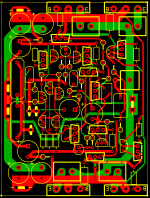
When you connect tracks on the PCB you should not create included angles less than 90 degrees, as in the example marked with an 'x'.
These can cause etchant to be trapped at the washing stage and cause problems with boards in later life. While this is a minor point, you should not see features like this on a professionally designed board.
Component outlines should NOT overlap as at 'y', the components should be drawn at the EXACT size. Then if the outlines overlap, the components themselves will clash or be trying to occupy the same space, which is obviously not possible.
In general, tracks should run horizontally, vertically and at 45 degrees with mitres to change direction.
w
Like this:
An externally hosted image should be here but it was not working when we last tested it.
Not like this:
An externally hosted image should be here but it was not working when we last tested it.
When you connect tracks on the PCB you should not create included angles less than 90 degrees, as in the example marked with an 'x'.
An externally hosted image should be here but it was not working when we last tested it.
These can cause etchant to be trapped at the washing stage and cause problems with boards in later life. While this is a minor point, you should not see features like this on a professionally designed board.
Component outlines should NOT overlap as at 'y', the components should be drawn at the EXACT size. Then if the outlines overlap, the components themselves will clash or be trying to occupy the same space, which is obviously not possible.
In general, tracks should run horizontally, vertically and at 45 degrees with mitres to change direction.
An externally hosted image should be here but it was not working when we last tested it.
w
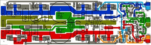
Grounding is the BIGGEST factor in final results. PMA (member) alerted me to the downfall of larger decoupling caps on the main board and how they "infect" the signal ground even if isolated with the usual 10-22R /double diode "isolation".
The simple solution is the split ground(G1 - G2). Geez , one more green wire (pix1 below) is not a bad price to pay for your small signal devices not to get "slammed" with a dirty ground. At the main power supply one can even isolate the separate clean ground with an inductor/resistor combo. As you can see below (Vee2 /Vcc2- pix2), I can even go "fanatic" and just use a separate supply for the "little stuff" leaving the power stage to sit in the foul cess of dirty power-ground all by it's self. But for a single supply setup the above scheme is the best . BTW , the simple cap multipliers will tame that 2-3v ripple at the main rails down to 5-10mv before they reach those blue/red LED's (power for voltage/input stage)") .
.
OS
The simple solution is the split ground(G1 - G2). Geez , one more green wire (pix1 below) is not a bad price to pay for your small signal devices not to get "slammed" with a dirty ground. At the main power supply one can even isolate the separate clean ground with an inductor/resistor combo. As you can see below (Vee2 /Vcc2- pix2), I can even go "fanatic" and just use a separate supply for the "little stuff" leaving the power stage to sit in the foul cess of dirty power-ground all by it's self. But for a single supply setup the above scheme is the best . BTW , the simple cap multipliers will tame that 2-3v ripple at the main rails down to 5-10mv before they reach those blue/red LED's (power for voltage/input stage)
.OS
Attachments
Sorry I tried to reply earlier on my phone and didnt realize that I just replied to the email
To Knatta:
I didn't think about having through hole stuff poke out underneath other components. That will make assembly much more difficult now that I think about it, I'll have to solder same side as a component... I'll go fix those.
To everyone:
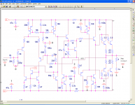
The reason the schematic is funny is because of the software I've not used before and it was hard to create, I'll post an updated version using orcad or something, hopefully tonight. I thought that I had to use their software but apparently I didn't so I redrew it all for nothing... Laaame.
I'll try to work out the references on the new schematic so it's easier to look at.
To WakiBaki:
I thought that looked a little funny but I thought it might be ok since they're all going to a single pad, I will work to get rid of these even when they are moving to pads. I started doing everything at 45Degrees but It got complicated at the end and I just got lazy. I'll fix it.
The Silkscreen overlaps because of my statement in the first post, I will be placing those caps on the back side. I forgot to include the NFB and Bias caps in the list. My bad, It shoulnd't interfere when im finished. Is there a way to show that in the schematic? I think they just have 1 silkscreen layer...
Leon
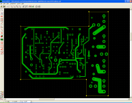
Grounds in the center. Quick topology discussion. Inputs on the left, ground is in center, V+ is top right, V- Bottom Right. Speaker ground and power ground are attached as they come into the quick connect to try and remove those currents from the board. Maybe have two quick connects side by side if I can make them fit.
Devils dance:
I tried to put the output caps by the output transistors but I can get them closer if you think they need to be.
Ostripper:
I tried to seperate the grounds, I attempted to create a star ground in the center of the board. It has only the signal and NFB grounds from the left. The Small signal cap grounds from below, and the output cap and CCs's grounds from the right.
I further was going to attach the speaker ground and the power ground from the power supply to the board together using the crimp from the quick connect, to try to islolate those currents from the board all together.
I have a split ground (3x) on my standard board right now but I was hoping to get rid of that by cleverly doing the above... Do you believe this to be insufficient? or non Ideal? It sounds like you do, and I'd be linclined to believe you.
Thank you for all the input these are all great sugesstions! I will give an update soon I hope.
To Knatta:
I didn't think about having through hole stuff poke out underneath other components. That will make assembly much more difficult now that I think about it, I'll have to solder same side as a component... I'll go fix those.
To everyone:
The reason the schematic is funny is because of the software I've not used before and it was hard to create, I'll post an updated version using orcad or something, hopefully tonight. I thought that I had to use their software but apparently I didn't so I redrew it all for nothing... Laaame.
I'll try to work out the references on the new schematic so it's easier to look at.
To WakiBaki:
I thought that looked a little funny but I thought it might be ok since they're all going to a single pad, I will work to get rid of these even when they are moving to pads. I started doing everything at 45Degrees but It got complicated at the end and I just got lazy. I'll fix it.
The Silkscreen overlaps because of my statement in the first post, I will be placing those caps on the back side. I forgot to include the NFB and Bias caps in the list. My bad, It shoulnd't interfere when im finished. Is there a way to show that in the schematic? I think they just have 1 silkscreen layer...
Leon
Grounds in the center. Quick topology discussion. Inputs on the left, ground is in center, V+ is top right, V- Bottom Right. Speaker ground and power ground are attached as they come into the quick connect to try and remove those currents from the board. Maybe have two quick connects side by side if I can make them fit.
Devils dance:
I tried to put the output caps by the output transistors but I can get them closer if you think they need to be.
Ostripper:
I tried to seperate the grounds, I attempted to create a star ground in the center of the board. It has only the signal and NFB grounds from the left. The Small signal cap grounds from below, and the output cap and CCs's grounds from the right.
I further was going to attach the speaker ground and the power ground from the power supply to the board together using the crimp from the quick connect, to try to islolate those currents from the board all together.
I have a split ground (3x) on my standard board right now but I was hoping to get rid of that by cleverly doing the above... Do you believe this to be insufficient? or non Ideal? It sounds like you do, and I'd be linclined to believe you.
Thank you for all the input these are all great sugesstions! I will give an update soon I hope.
Last edited:
Hopefully not offending anyone (mainly women), but thats damn sexy! Not only is it mostly one sided but the program looks nice too, what is that software ur using?
Unfortunately I have to have all the outputs on one side for my design to work right now but I will look into a way to make it work otherwise. I didn't originally think I could make it near as compact as this so I might be able to work around my original constraints.
I'll have to look at that design more closely, hopefully you didn't go and design it just for me, but I thank you if you did.
Just a few ideas:
You shouldn't draw connections over components in you schematic. This makes the schematic hard to read and very confusing.
Overall design is very confusing (not a good sign). I can't tell whether you got it right. Missing reference designators make is hard to compare the pcb design with the schematic.
To reduce problems you really need a pcb cad packgae that has lots of error checking. i.e. lines under pins, single ended nets, unconnected pin scan in schematic.
i.e. clearance check, continuity check, min via size check, track layers out of range in pcb.
You don't need both grounds 3 and 4 - the zobel network can share the output ground. OTOH the input ground and the input RC filter ground would be better off not being the same. Input cable screens act as excellent antennas which in this case would inject RF into the input via the 220pF. So re-allocate ground 3 to the input - that is ground 0.
Last edited:
...this weekend I spend some time in front of my monitor and PCB are ready ??
Regards Alex .
What layout program do you use to do this FANTASTIC work?
Thanks if for nothing else but aspiration to come close to this professional work...
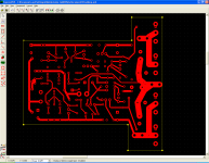
I have an updated schematic. I'm attempting to make them as small as possible so that I can keep the cost down. Plus this allows me to use the heat sinks as efficiently as possible. Does anyone think that using separate heat sinks for the upper and lower transistors would be a problem?
The problem is that 4 transistors per heat sink (side by side) is really cramming them on. 2x2 is a much better configuration, but I cant get them close enough on a single board because I would have to mount them through the board... I guess its possible, but I would rather not.
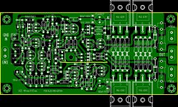
I've tried to incorporate the suggestions to this board and condense it to be even smaller. What are your thoughts?
The problem is that 4 transistors per heat sink (side by side) is really cramming them on. 2x2 is a much better configuration, but I cant get them close enough on a single board because I would have to mount them through the board... I guess its possible, but I would rather not.
I've tried to incorporate the suggestions to this board and condense it to be even smaller. What are your thoughts?
Attachments
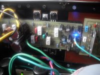
.....last PCB adjusted to final schematic
Dear Alex,
Wonderful work. One advice though for even lower THD. In your design you run the loudspeaker output in the middle, the PSU lines on the outer side, and the small line signal that feeds the transistors between the PSU line and the output. This way the line input signal line is burried between the magnetic field of the output and PSU lines. Why not run the PSU lines inwards close to the output line, and route the line signal level lines outwards?
Also the de-coupling caps should have a very short ground-trace. In your design they have a very long trace to ground, which kinda reduce their working inductive wise. Ideally they are connected close together and share a very short ground trace.
With kind regards,
Bas
Last edited:
you think like Doc Cherry and I try to adopt......... you run the loudspeaker output in the middle, the PSU lines on the outer side, and the small line signal that feeds the transistors between the PSU line and the output. This way the line input signal line is burried between the magnetic field of the output and PSU lines. ................. de-coupling caps should have a very short ground-trace. In your design they have a very long trace to ground, which kinda reduce their working inductive wise. Ideally they are connected close together and share a very short ground trace.
- Status
- This old topic is closed. If you want to reopen this topic, contact a moderator using the "Report Post" button.
- Home
- Amplifiers
- Solid State
- PCB Layout Questions