Thanks for the clarification--I thougth so, but I'd have called this "source impedance", so I wasn't sure.
Maybe I'm off here, but is this effect not more like an output conductance effect? It looks to me as if the drain resistor were replaced with an active transimpedance stage (opamp IV-converter), the effect would not be observed. However, if it were indeed attributed to transconductance, there would be no sensitivity to the drain load impedance.
Samuel
Hi Samuel,
This is a good question. I think it could possibly also be modeled as an output conductance, since my observation of reduced output current available to the load resistor was in fact a function of the output voltage. We might want to look at this further. I think the output conductance might end up being a fairly significant and unexpected amount of conductance, but such a model might be just as valid as the voltage and frequency dependent gm effect that I modeled it as.
Just thinking out loud, maybe we could distinguish the effect of transconductance vs output conductance by comparing differences in the effect when in the common source vs common drain modes of operation. For example, perhaps we look at the output impedance of the source follower under the different operating point and frequency conditions. More thought is obviously required.
Cheers,
Bob
Hi dado,
I've used both BJT and HEXFET MOSFETs with success for these current sources. It is, of course, important that they have adequate voltage, current, dissipation and SOA ratings for the application.
Cheers,
Bob
Yes I know that. In the case of those Supertex Deplation-Mode(normally-on) MOSFETs there is adequate voltage(250-300V) current(Idss 150mA) dissipation(1W, 15W) and for excellent CCS you need one MOSFET and one resistor.
dado
Yes I know that. In the case of those Supertex Deplation-Mode(normally-on) MOSFETs there is adequate voltage(250-300V) current(Idss 150mA) dissipation(1W, 15W) and for excellent CCS you need one MOSFET and one resistor.
dado
Hi dado,
Yes, the use of the depletion mode MOSFETs is a cool idea and can result in a simple circuit. I must admit that I have not used depletion mode MOSFETs.
Cheers,
Bob
Hello Bob
In your expererience Bob what have you found to be the practical limit to how far down you can reduce the even order harmonics due to half wave currents caused in the ouput stage of a Class A/B amplifier at 20Khz.
Regards
Arthur
Hi Arthur,
This is a good question and of course subject to YMMV. In my MOSFET power amplifier with error correction I got to below 0.001% THD, and the influence of the half-wave class AB output currents was probably below that.
Getting the influence of those currents way down involves great care and attention to detail in layout. For example, when I use multiple output pairs, I interleave the P and N devices rather than group each sex together. This helps with some cancellation of the created magnetic fields. I also try to take advantage of the fact that in such amplifiers the sum of the positive and negative rail currents is essentially linear, so twisting together the + and - rail leads helps cancel the fields there. I also try to strongly AC short the positive and negative rail at the output stage with capacitors that straddle the rails in order to get those currents summed together as locally as possible.
It is also important to keep that influence away from the feedback path. I send the full-amplitude output signal back to close to the input stage, where I then have the feedback network.
It is also very important to pay attention to grounding and not allow these half-wave currents to corrupt the ground, espcially the quiet ground. Also be aware that power supply bypass capacitors can corrupt a ground by bypassing these half-wave rectified rail noises into the ground. Overall, grounding practices are very important in this regard.
Cheers,
Bob
better safe than sorry
And as a last resort, you may 'actively' compensate for the half-wave output currents. See my magic little pot P2 (10 Ohms) in: MCP Output Stage
(node out1 goes to the TMC network of the front-end)
Cheers,
E.
And as a last resort, you may 'actively' compensate for the half-wave output currents. See my magic little pot P2 (10 Ohms) in: MCP Output Stage
(node out1 goes to the TMC network of the front-end)
Cheers,
E.
Hi Arthur,
This is a good question and of course subject to YMMV. In my MOSFET power amplifier with error correction I got to below 0.001% THD, and the influence of the half-wave class AB output currents was probably below that.
Getting the influence of those currents way down involves great care and attention to detail in layout. For example, when I use multiple output pairs, I interleave the P and N devices rather than group each sex together. This helps with some cancellation of the created magnetic fields. I also try to take advantage of the fact that in such amplifiers the sum of the positive and negative rail currents is essentially linear, so twisting together the + and - rail leads helps cancel the fields there. I also try to strongly AC short the positive and negative rail at the output stage with capacitors that straddle the rails in order to get those currents summed together as locally as possible.
It is also important to keep that influence away from the feedback path. I send the full-amplitude output signal back to close to the input stage, where I then have the feedback network.
It is also very important to pay attention to grounding and not allow these half-wave currents to corrupt the ground, espcially the quiet ground. Also be aware that power supply bypass capacitors can corrupt a ground by bypassing these half-wave rectified rail noises into the ground. Overall, grounding practices are very important in this regard.
Cheers,
Bob
Hello Bob
Thankyou for your response, I notice that you dont rate 4 layer PCB as an essential element to solve the distortion mechanism am I correct in assuming this.
I like taking the full amplitude output signal right back to the input where you connect the feedback resistor network, is this so the feedback resistors are away from large currents which cause the magnetic fields , is a copper track less effected than a resistor body to these fields. I am going to implement this in my next amp .
Regards
Arthur
And as a last resort, you may 'actively' compensate for the half-wave output currents. See my magic little pot P2 (10 Ohms) in: MCP Output Stage
(node out1 goes to the TMC network of the front-end)
Cheers,
E.
Hello Edmond,
I like this idea, but I notice in the circuit you have two outputs which are summed and integrated into your amp , how would I sum them in the circuit you know I have built , I dont use a current feedback input.
Regards
Arthur
Hi Arthur,
It's fairly simple. You can do it with any amp. In case of TMC it's even simpler: just tie the resistor of the TMC network not directly to the output, but rather to the wiper of the magic pot instead.
Cheers,
E.
BTW, did you read the story of the EF50 (at everything else) ?
It's fairly simple. You can do it with any amp. In case of TMC it's even simpler: just tie the resistor of the TMC network not directly to the output, but rather to the wiper of the magic pot instead.
Cheers,
E.
BTW, did you read the story of the EF50 (at everything else) ?
Hi Arthur,
[snip]It is also important to keep that influence away from the feedback path. I send the full-amplitude output signal back to close to the input stage, where I then have the feedback network.[snip]Cheers,
Bob
Hi Bob,
This is an interesting view point. I have always placed the fb resistor directly at the output so that the feedback signal going back to the input stage was low-level. My reasoning is that that minimizes any unwanted coupling of the large output signal to relative sensitive stages towards the input.
jan didden
Bob's approach was also recommended by Morgan Jones in Building Valve Amplifiers. His approach was a shielded twisted pair from the output to the feedback series resistor, with the other wire attaching directly to the bottom of the feedback shunt resistor, and the shield connected to ground at the driving end only.
Hi Bob,
This is an interesting view point. I have always placed the fb resistor directly at the output so that the feedback signal going back to the input stage was low-level. My reasoning is that that minimizes any unwanted coupling of the large output signal to relative sensitive stages towards the input.
jan didden
Jan, if there is any coupling in the feedback line, the fb resistor would attenuate the coupled signal also if it is at the input end. Also, if the output coupling is magnetically induced, wouldn't it couple better to a low impedance path? If the fb resistor is placed at the output end, the fb line would have a lower impedance back to the input stage, the impedance being effectively the lower shunt resistor absent the series resistor.
Also, if noise is coupled to a signal line, wouldn't it have a better S/N ratio if the signal voltage is larger (i.e., not attenuated first)?
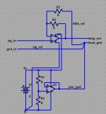
I drew this for headphone amps with active gnd but I think the location of the star gnd is relevant for common impedance coupling
magnetic coupling would appear to be made more linear if the +/- power trace is "common centroid" or low loop area - interleaving N/P output Q physical positions may drive assembly people nuts but may be "better" from this perspective
magnetic coupling would appear to be made more linear if the +/- power trace is "common centroid" or low loop area - interleaving N/P output Q physical positions may drive assembly people nuts but may be "better" from this perspective
Attachments
Bob's approach was also recommended by Morgan Jones in Building Valve Amplifiers. His approach was a shielded twisted pair from the output to the feedback series resistor, with the other wire attaching directly to the bottom of the feedback shunt resistor, and the shield connected to ground at the driving end only.
Yes, if you follow Bob's approach a screened cable would make sense.
But it isn't really necessary with the other approach.
jan didden
Jan, if there is any coupling in the feedback line, the fb resistor would attenuate the coupled signal also if it is at the input end. Also, if the output coupling is magnetically induced, wouldn't it couple better to a low impedance path? If the fb resistor is placed at the output end, the fb line would have a lower impedance back to the input stage, the impedance being effectively the lower shunt resistor absent the series resistor.
Also, if noise is coupled to a signal line, wouldn't it have a better S/N ratio if the signal voltage is larger (i.e., not attenuated first)?
Yes all good questions. In my view the thing to watch out for is coupling from the output signal to sensitive input circuits.
If you are more worried about something externally coupling into the fb line, you choices might be different.
I've been bitten by oscillations due to unwanted signal coupling, I haven't had any problems with external stuff coupling in, so that may explain my preference.
jan didden
Hello Bob
Thankyou for your response, I notice that you dont rate 4 layer PCB as an essential element to solve the distortion mechanism am I correct in assuming this.
I like taking the full amplitude output signal right back to the input where you connect the feedback resistor network, is this so the feedback resistors are away from large currents which cause the magnetic fields , is a copper track less effected than a resistor body to these fields. I am going to implement this in my next amp .
Regards
Arthur
Hi Arthur,
4-layer PCBs can be really helpful in all sorts of issues in power amplifiers, but I would stop short of rating them as essential in solving the class-AB magnetic distortion problem. They can certainly help, however.
BTW, I use 20-layer PCBs where I work
") .
.My suggestion of routing the full-amplitude output signal back to a feedback network that is in close proximity to the input stage is mainly because a given amount of noise induced in to a line carrying a higher voltage will have a lesser percentage effect.
Cheers,
Bob
Hi Bob,
This is an interesting view point. I have always placed the fb resistor directly at the output so that the feedback signal going back to the input stage was low-level. My reasoning is that that minimizes any unwanted coupling of the large output signal to relative sensitive stages towards the input.
jan didden
Hi Jan,
This is also a valid way of looking at it. One is an issue of magnetic coupling while the other is an issue of capacitive coupling. I think it is easier to minimize the capacitive coupling, resorting even to guard traces if desired. Perhaps more importantly, that which is being coupled in from the output lead is linear as opposed to the magnetic garbage being nonlinear and distortive.
Cheers,
Bob
My suggestion of routing the full-amplitude output signal back to a feedback network that is in close proximity to the input stage is mainly because a given amount of noise induced in to a line carrying a higher voltage will have a lesser percentage effect.
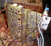
In light of this , would (below 1) be okay ? Or would a shielded cable be better.
Purple wire (NFB L/R) only crosses low imp. areas. Rails are at the sides (orange/red). BTW , that is the TMC'ed "bobamp" (or blameless).
OS
Attachments
- Home
- Amplifiers
- Solid State
- Bob Cordell's Power amplifier book