That solder requires a higher temp to melt, putting more stress on the component.I use lead free solder, to ensure ROHS.
You do not need to be worried about ROHS compliance, you are not selling anything, it is a hobby, you are exempt imo.
Think of it as inter stellar rocket science
") I do not think NASA gives two hoots about ROHS compilance. ROHS is meant for throw away electronics.
I do not think NASA gives two hoots about ROHS compilance. ROHS is meant for throw away electronics.For the SOT6, there are two different manufacturers for the 5551, but they have different footprints. I am not too bothered about the power aspect - as i only use them in low power parts of the circuit.
For others who might have different plans I have seen instances of pcb layout having enlarged areas of copper near small signal transistors allowing heat transfer route away from the die via lead connections.
While that strategy would add an unknown collector to base capacitance in a VAS stage, the added component Miller capacitor was a lowly 39pF in one case I have seen.
Unlikely I think. Thermal stress in operation fatigues bonding wires due to the expansion/contraction of the epoxy. Running them hot is more of an issue than soldering them in the first place as fatigue is a cyclic thing.Hi rsavas,
Thanks - I can only assume it is the pressure i am placing on the component. I use the same method as yourself, one pad used to secure the device and then opposite corner to ensure the IC is level. I use lead free solder, to ensure ROHS.
thats odd then, transistors should just work reliably run cool.For the SOT6, there are two different manufacturers for the 5551, but they have different footprints. I am not too bothered about the power aspect - as i only use them in low power parts of the circuit.
Is your iron temp control working properly?
Reflow oven for me, quick and neat and no mess.Hi Mark J,
I have a hot air station - but preference is for hand soldering using a soldering iron - it is just as fast to implement.
Regards,
Shadders.
Hi Bob,
I have been reading through chapter 2 of your second edition and must say, I have really enjoyed the new content and explanations you have provided. It has really help me get a better understanding.
I have a question that I was hoping you or another member could help me with.
At the bottom of page 30 in the paragraph below the formula labeled (2.14)
You talk about how the early effect is mitigated by the use of emitter degeneration.
What I was having trouble understanding is. You say that "most of the signal current flowing in ro is returned to the collector by way of being injected into the emitter."
My question and lack of understanding is. How does the signal current return to the collector if the current is already flowing from collector to emitter?
Hi Bob,
I have been reading through chapter 2 of your second edition and must say, I have really enjoyed the new content and explanations you have provided. It has really help me get a better understanding.
I have a question that I was hoping you or another member could help me with.
At the bottom of page 30 in the paragraph below the formula labeled (2.14)
You talk about how the early effect is mitigated by the use of emitter degeneration.
What I was having trouble understanding is. You say that "most of the signal current flowing in ro is returned to the collector by way of being injected into the emitter."
My question and lack of understanding is. How does the signal current return to the collector if the current is already flowing from collector to emitter?
With a highly degenerated emitter, most of the current flowing through ro will flow into the emitter rather than into the emitter degeneration resistor. This decreases the net emitter current by almost the amount of current flowing in ro. Thus, the current flow being referred to is in the form of lessened emitter and collector current. This tends to cancel the current that was effectively flowing as collector current through ro. This effect workes especially well when beta of the transistor is high and the base is driven from a low-impedance source, such as an emitter follower. This is one reason why a degenerated 2T VAS is quite good, and has a fairly high output impedance.
If you have a VAS operating at 10 mA, its re' is about 2.6 ohms. If you then degenerate it with 26 ohms, about 90% of the current through ro will flow into the emitter and tend to cancel the increased collector current caused by ro. This is also one reason why the product of early voltage and beta of a VAS transistor (figure of merit) can be important to overall VAS performance.
Cheers,
Bob
Thanks for the extra explanation and clarification on that topic Bob. I really appreciate your time and support.With a highly degenerated emitter, most of the current flowing through ro will flow into the emitter rather than into the emitter degeneration resistor. This decreases the net emitter current by almost the amount of current flowing in ro. Thus, the current flow being referred to is in the form of lessened emitter and collector current. This tends to cancel the current that was effectively flowing as collector current through ro. This effect workes especially well when beta of the transistor is high and the base is driven from a low-impedance source, such as an emitter follower. This is one reason why a degenerated 2T VAS is quite good, and has a fairly high output impedance.
If you have a VAS operating at 10 mA, its re' is about 2.6 ohms. If you then degenerate it with 26 ohms, about 90% of the current through ro will flow into the emitter and tend to cancel the increased collector current caused by ro. This is also one reason why the product of early voltage and beta of a VAS transistor (figure of merit) can be important to overall VAS performance.
Cheers,
Bob
Adding to my above post, I can see from the formula ro = (VA + Vce) / Ic
how adding a VAS cascode transistor would also help to stabilize the value of ro as the value of Vce does not vary as much when a VAS cascode transistor is used. So I guess this is one of the reasons it helps with reducing amplifier non linearities.
how adding a VAS cascode transistor would also help to stabilize the value of ro as the value of Vce does not vary as much when a VAS cascode transistor is used. So I guess this is one of the reasons it helps with reducing amplifier non linearities.
Adding to my above post, I can see from the formula ro = (VA + Vce) / Ic
how adding a VAS cascode transistor would also help to stabilize the value of ro as the value of Vce does not vary as much when a VAS cascode transistor is used. So I guess this is one of the reasons it helps with reducing amplifier non linearities.
Try read this
https://www.passlabs.com/sites/default/files/cascode.pdf
Thanks jony. That was a good read both from the perspective of the advantages of cascodes and some of the problems that arise from large amounts of gain and large amounts of negitive feedback etc.
I have not read alot about Nelson's amplifiers as I thought that they were all class A. I would however be interested to read a little more about simlar circuit topologies. Do you have a link to any of Nelson's amplifiers that share that topology that I could read a little more on?
https://www.diyaudio.com/forums/sol...lls-power-amplifier-book-754.html#post4909328@Bob
Have you ever seen this used anywhere? ....
https://www.diyaudio.com/forums/pass-labs/262821-class-ap-amplification.html#post4077413
https://www.diyaudio.com/forums/att...103312011-crossover-distortion-hartsuiker-jpg
I find a bit puzzling that the impedance seen by the emitters of the common base transistors is much lower in Hartsuiker's amplifier than in Blomley's amplifier.
Hi all,
First let me say that I am aware that this is a bit off-topic in this thread.
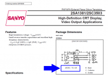
However, knowing that the 2SC3503 has been discussed here, and also in Bob's book, I reckon some of you know what it should look like ... so I hope you will excuse my brief digression ..
As it is I recently bought some 2SC3503's that should be genuine Sanyo transistors. But checking Sanyo's datasheet on this transistor it does not appear to have a metal backside for cooling - which the ones I have bought have (photo attached).
Might one of you confirm or dismiss that these are genuine Sanyo 2SC3503s?
Cheers & thanks (and again pardon me for the digression),
Jesper
First let me say that I am aware that this is a bit off-topic in this thread.
However, knowing that the 2SC3503 has been discussed here, and also in Bob's book, I reckon some of you know what it should look like ... so I hope you will excuse my brief digression ..
As it is I recently bought some 2SC3503's that should be genuine Sanyo transistors. But checking Sanyo's datasheet on this transistor it does not appear to have a metal backside for cooling - which the ones I have bought have (photo attached).
Might one of you confirm or dismiss that these are genuine Sanyo 2SC3503s?
Cheers & thanks (and again pardon me for the digression),
Jesper
Attachments
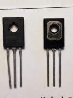
Hi,As it is I recently bought some 2SC3503's that should be genuine Sanyo transistors. But checking Sanyo's datasheet on this transistor it does not appear to have a metal backside for cooling - which the ones I have bought have (photo attached).
Might one of you confirm or dismiss that these are genuine Sanyo 2SC3503s?
Funnily, i was looking at some youtube videos of fake IC's etc., and the picture indicates tinning of the leads of the transistor, which indicates that they may be fake components.
Did you purchase from ebay ?.
I searched on the component, and the Fairchild version should be available from Mouser or other source. (KSC3503)
I personally would never purchase from ebay.
Regards,
Shadders.
Last edited:
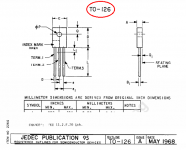
If you investing the to-126 package you will find that it has a metal plate. The KSC3503 is in a to-126ML package which is isolated and thicker. I bought some 2sc3503 from eBay polida that look to be genuine, the metal tabs are oxidized so show there age. I have yet to test them
Hi,I bought some 2sc3503 from eBay polida that look to be genuine, the metal tabs are oxidized so show there age. I have yet to test them
One video i viewed was about polida 2008 username :
YouTube
Time 00:14 shows the name, and 14:46 approx is the summary.
I suppose, YMMV.
Regards,
Shadders.
Yes I have heard the same but one wonders who you can trust as being correct. I have bought parts from polida that I know are genuine but I can not say that for everything they sell even these 2sc3503 until I test them. Buyer beware
Fairchild should have said there package is not a true to-126 by Jedec definition and a variation to not cause this confusion
Fairchild should have said there package is not a true to-126 by Jedec definition and a variation to not cause this confusion
Last edited:
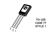
JEDEC standard package TO-126 has no metal tab for heatsinking. You are thinking of JEDEC standard package TO-225.
Fairchild's copycat parts KSC3503 are also packaged in TO-126.
_
Fairchild's copycat parts KSC3503 are also packaged in TO-126.
_
Attachments
Last edited:
...
As it is I recently bought some 2SC3503's that should be genuine Sanyo transistors. ...
Looks like the fakes I have bought years ago:
2SC3503+2SA1381 E or F source?
BR, Toni
Yes I am confused. I do see that Sanyo has the thickness as 2.7mm & Fairchild has it as 3.05-3.45mm so they do not agree so who is correct? I know the to-126 heatsinks I am using are a PITA to put on the Fairchild package so I wonder if it meet the jedec outline. Can you post the complete Jedec spec for me to look at?
Now that Toni weighs in I am questioning those parts I bought from polida too
Now that Toni weighs in I am questioning those parts I bought from polida too

- Home
- Amplifiers
- Solid State
- Bob Cordell's Power amplifier book