It took me less than 1 second and Google. How were you searching???
http://www.datasheetarchive.com/2SC1663-datasheet.html
http://www.datasheetarchive.com/2SC1663-datasheet.html
Yes had those site too. Its informs about all characteristics, but no pinout visible , for me at least.
I saw on that site that it was package TO-202var, so then put that into Google and found another device with that pinout and a datasheet for it.
<<Then is the layout printed allright in the service manual, but not correct on the pcb.>>
Too bad. I wouldn't be surprised, if you will end up with this pinout: B-C-E.
Collector voltage drop will be less then that of the Emitter junction. And you can follow the traces on the board.
For replacement look for the same grades: Sony grades their parts by digits.
Too bad. I wouldn't be surprised, if you will end up with this pinout: B-C-E.
Collector voltage drop will be less then that of the Emitter junction. And you can follow the traces on the board.
For replacement look for the same grades: Sony grades their parts by digits.
I am searching for the pin order of these transistors. Searched some while on www no result.
Anyone?
SONY 2SA835 can replace through Motorola MPS-U60
SONY 2SC1663 can replace through Motorola MPS-U10
pinout and outline is the same by all types - go to
http://pdf1.alldatasheet.com/datasheet-pdf/view/124196/MOTOROLA/MPS-U10.html
http://pdf1.alldatasheet.com/datasheet-pdf/view/100844/MOTOROLA/MPS-U60.html
This information I read in the same order by follow comparsion table books in German Language
1) ECA "tvt transistoren2 '79/80
2) JAEGER ELEKTRONIK Vergleichstabelle 2001
Last edited:
tubee,
Anyway, it`s going to be a degrade not an upgrade.

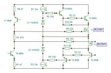
Nice devices in a nice configuration. Are you sure that all of them are defective?Sony Vfets 2SJ18/2SK60 cascaded with transistors.
Anyway, it`s going to be a degrade not an upgrade.
I am busy with this beast for a year now. 1 fet was burned and 2 drivertransistors and 1 cascaded transistor.
I replaced the cascade transistors to heavier ones, they are the cause of Vfet failure, and want to prevent expensive obsolete Vfet frying again.
All caps are replaced except the big Lytics, all fusible resistors and some diodes/zeners.
So if someone has (a supplier for) Nippon Chemicon 27000uF/80V lytics.
An externally hosted image should be here but it was not working when we last tested it.
I rather like to keep the Vfets.
Well i have done all work right, the Sony is revived again after so many years.
An externally hosted image should be here but it was not working when we last tested it.
tubee,
congratulations.
congratulations.
Of course.I rather like to keep the Vfets.
A different brand should do as well, the higher capacitance the better.So if someone has (a supplier for) Nippon Chemicon 27000uF/80V lytics
- Status
- This old topic is closed. If you want to reopen this topic, contact a moderator using the "Report Post" button.
- Home
- Amplifiers
- Solid State
- Searching pinout 2SC1663/2SA835