Yep. 1000VA total will be more than adequate. Most off the shelf recievers will probably only use 500VA total!
It depends what you're doing - I'd assumed 5.1. Personally I think with good front speakers, a centre speaker isnt neccesary, but thats just me") You could easily make a small mixer circuit to mix a centre output into front left/right
You could easily make a small mixer circuit to mix a centre output into front left/right
It depends what you're doing - I'd assumed 5.1. Personally I think with good front speakers, a centre speaker isnt neccesary, but thats just me
You could easily make a small mixer circuit to mix a centre output into front left/rightAssuming you don't need any gain, just attenuation, then it's implemented as simply as a potentiometer wired up as a potential divider. Typically 47K log pots are used although everything from 10K-100K is used depending on the circuit.
In this particular application, I dont know what your source will be - presumably a DVD player with 6 channel outputs. You might want to use an opamp connected as a simple buffer before the pots.
In this particular application, I dont know what your source will be - presumably a DVD player with 6 channel outputs. You might want to use an opamp connected as a simple buffer before the pots.
six buffers to feed the 6channel volume control and six buffers after the volume control to feed the six interconnects.jaycee said:a DVD player with 6 channel outputs. You might want to use an opamp connected as a simple buffer before the pots.
I think that 4.1 will be more than adequate.
I am assumeing you either have 6 (5.1)discrete outputs out of your DVD player or 5.1 decoder. Its best to have 5 seperate amps and speakers, but if you can only build 4 amps your surrounds will have to be a summed mono of the 2 surround outputs. The centre channel in the front is where most of the dialogue comes from so you cant just loose it.
I see your point.
Okay then....slowly I will begin construction of 6 boards.
so for now the plan is like so:
1) 2 toroidals 500va
2) 6 33,000uf + *bucket* of 4700uf
3) 5.1 channels
4) no preamp
and for the tricky( for me ) bits
5) attenuation
6) motororised attenuation? startup?
7) a good softstart circuit.....before or after the 220v filter?
P.s. what are the exact dimensions of the quasi nmos 200? I usually check with the board desginer for the exact measurments so I can set them directly in the viewer software in order to print the master. Can you tell me what these measurements are?
The filter should come first. If you buy an IEC connector with built-in filter, there is actually not even a choice. Look for a filter that matches the actual current consumption. Bigger is not better in that case.Alexontherocks said:7) a good softstart circuit.....before or after the 220v filter?
this is the project I intend to use. the toroid filter will be a current compensated epcos toroid good for 8A at 230v
An externally hosted image should be here but it was not working when we last tested it.
When you design a filter there are two things to consider about current.
One is the current rating. E. g. a toroid like yours will not necessarily be damaged by a current that is higher than 8 A. It will saturate and produce harmonics instead of filtering them out. To avoid that, the highest current that is usually drawn, should remain below that rating.
The second is the filter curve. Mains filters are low-pass filters. If you design a filter, you usually know the load that will be present. E. g. if you design the input filter for an amplifier you know the input resistor size and can easily calculate the capacitor for a certain frequency. The current consumption of an amplifier is however not constant, so the filter frequency will be changing all the time. The corner frequency will be higher, when the current is high than when it is low. If you use a filter that is designed for too high a current, it is possible that its corner frequency falls too low, when little current is drawn. The filter will start to act on the 50 Hz or 60 Hz mains frequency and convert some of the energy into heat.
Commercial filters are usually 12 dB filters. If you design your own filter, go for a steeper one, e. g. 24 dB. Find out the lowest current the amplifier draws and set the filter so that it starts to act just above the mains frequency with that load.
E. g. your schematic shows a current compensated choke, but no value is given, so we do not know, at which frequency it acts. After the choke there is a 150 nF capacitor. You mentioned 8 A, which corresponds to 28,75 Ohms at 230 V. The corner frequency of that capacitor will be ~37 kHz. If the lowest current was 0,1 A, which would correspond to 2,3 kOhms, you get a corner frequency of 460 Hz and you could use a bigger capacitor to bring that further down, maybe to 100 Hz or so.
Of course you have to do the math for the entire filter including the choke. The above was just to make the idea clear, why a mains filter should be matched to the load, not oversized.
One remark to your schematic. You have drawn the windings of the choke connected in opposite directions. Although that is electrically correct, the windings of current compensated chokes are usually drawn in the same direction and the input sides are marked with a dot to show that they work in opposite directions.
Alexontherocks said:P.s. what are the exact dimensions of the quasi nmos 200? I usually check with the board desginer for the exact measurments so I can set them directly in the viewer software in order to print the master. Can you tell me what these measurements are?
The Nmos200 PCB is 90mm long x 75mm wide. You will need to add about 3-5mm in the length for the heatsink bracket depending on what you will use.
Cheers
Quasi
Quasi! I was just about to email you with some questions but thought that you wouldn't be interested in trivial matters like this. I did not want to bother you.
As you can see I am planning out my build. If everything goes as planned I will effectively have a total of over 600,000uf for 6 channels, 1500va of transformer power (at 36v dual output) and of course your great other projects:
the dc protection and softstart.
I am relieved that the dimensions are just what I expected. I will certainly be able to fit 2 on one eurocard and save space inside the casing (which is a very large full aluminium car amplifier case designed to house a top of the line 600w rms 1ohm amplifier).
Hopefully in a few weeks time I will able to set up a page on the internet and describe everything. All necessary credit will be given to the designers of each circuit I will use.
Alex
P.s. of course credit shall be given to this great forum and the helpful members who have answered my thread.
Hi everyone. I just finished making the pcbs for the amplfiier (6 quasi nmos200) and 6 pcb designed to hold 16 caps each.
If I wanted to avoid the shorcircuit effect during initial charge can I place 5w 1O resistors across the terminals of every cap?
IF any other solution is to be preferred please tell me.
Thanks
Alex
P.s. I also printed other 4 boards so I can assemble a smaller amplifier. 4 channels.
If I wanted to avoid the shorcircuit effect during initial charge can I place 5w 1O resistors across the terminals of every cap?
IF any other solution is to be preferred please tell me.
Thanks
Alex
P.s. I also printed other 4 boards so I can assemble a smaller amplifier. 4 channels.
You would not avoid the short circuit effect as the current would take the easier path through the discharged caps.
You might need to build a sequenced supply if you have trouble with powering 5 channels from cold at once. You could probably switch the rails with low RDSon mosfets rather than relays. With a background in power supplies I expect this is easy for you
You might need to build a sequenced supply if you have trouble with powering 5 channels from cold at once. You could probably switch the rails with low RDSon mosfets rather than relays. With a background in power supplies I expect this is easy for you
thanks for all your help. I will look into the problem in a few days.
For now I have been completing the capacitor banks.
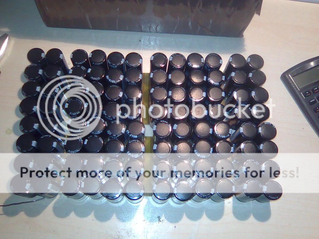
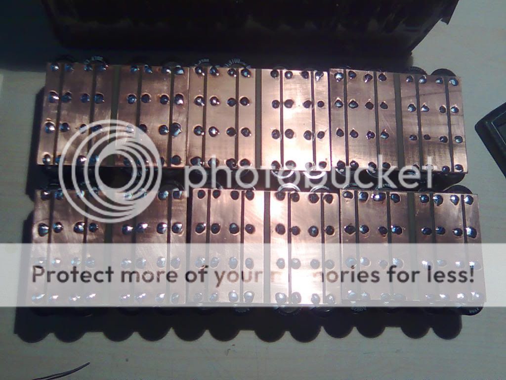
Here are the photos of 96 4700uf caps on 6 boards.
I will use bridges to connect the 2 independent set of tracks on the solder side. From there I will then merge the banks by soldering heavy duty wiring.
However I have a question.
How should I hook up all my caps?
The problem is that I have 6 33000uf and 96 4700uf. 3 toroidals and 3 rectifiers. Since voltages from the various toroids are slightly different I must keep them separated.
I have therefore 3 sets of leads (ffrom rectifier 1, from rectifier 2 and from rectifier 3).
I was thinking of dividing al my capacitors equally ending up ideally with this kind of setup (multiplied by 3 therefore each powering two channels)
toroid - 2x33000uf caps - 2x 16x4700uf caps - power connector.
Also if this all correct do you suggest I add more caps with smaller capacity to increase response when playing high frequencies?
the 1F goal is very tempting.
P.s. I work slow but rest assured I am going to complete this project. Right now all my amp boards are ready to be assembled but before I'd rather complete the "power" module so I can test any amp I assemble.
Alex
For now I have been completing the capacitor banks.
Here are the photos of 96 4700uf caps on 6 boards.
I will use bridges to connect the 2 independent set of tracks on the solder side. From there I will then merge the banks by soldering heavy duty wiring.
However I have a question.
How should I hook up all my caps?
The problem is that I have 6 33000uf and 96 4700uf. 3 toroidals and 3 rectifiers. Since voltages from the various toroids are slightly different I must keep them separated.
I have therefore 3 sets of leads (ffrom rectifier 1, from rectifier 2 and from rectifier 3).
I was thinking of dividing al my capacitors equally ending up ideally with this kind of setup (multiplied by 3 therefore each powering two channels)
toroid - 2x33000uf caps - 2x 16x4700uf caps - power connector.
Also if this all correct do you suggest I add more caps with smaller capacity to increase response when playing high frequencies?
the 1F goal is very tempting.
P.s. I work slow but rest assured I am going to complete this project. Right now all my amp boards are ready to be assembled but before I'd rather complete the "power" module so I can test any amp I assemble.
Alex
let's assume you divide up all your capacitance equally between the three toroids.
You end up with +-108mF on each PSU.
That is about double what a ClassAB amplifier would have that has adequate smoothing or about the same as a big ClassA amplifier.
Do not worry about adding any more smoothing.
Look to decoupling at/on the amplifier PCB.
Look also at keeping the area of the transformer to rectifier cable loop as small as possible. Twisted pairs or twisted triplets for almost the whole route. Similarly keep the area of the rectifier to smoothing caps loop as small as possible.
These wires do not need to be large in cross sectional area.
The transformer and the connecting wires in combination with the capacitance form an rC filter. A little bit of extra r does no harm, it lowers the frequency of the low pass filter helping to attenuate the higher frequencies that come from the mains and the rectifiers.
If your secondary resistance is 0r5 and the reflected impedance from the primary is also 0.5ohms, you have r=1ohm.
If your cables from transformer to smoothing caps have a total resistance of 0r1 then the rC is 1r1 & 108mF.
If you double the area of your connecting cables to reduce the resistance by half, the rC becomes 1r05 & 108mF. I would advise the higher resistance cabling. It's cheaper, it's easier to fit and solder, it attenuates better, it is easier to twist right up to the terminals.
Finally fit a separate fuse to each transformer. Make this fuse rating as small as possible and yet allows the amplifier to perform faultlessly in the loudest setting you are ever likely to need. Maximum power into 4r0 is probably your worst case.
When you use so many capacitors in parallel, you should try to achieve the same path resistance to each capacitor. To achieve that you should not use the usual approach of having all inputs on one side of the board and all outputs on the other. The right way to do this is to have the ground input on one side and the rail inputs on the other side with the ouputs on the opposite sides.

The reason for this is that only low frequency ripple current divides according to capacity. High frequency ripple current divides according to resistance, i. e. ESR + trace resistance + wire resistance. And in a parallel configuration you want all the ripple current to divide equally among the capacitors so that none blows due to overload.
If you do it as in the schematic, the path from V+ IN to GND IN has more or less the same length through C1 as through C2 or C3 or C4. With the usual wiring, where GND IN would be on the right side, the path through C1 would be much shorter than through C4.
You have to maintain that concept throughout the entire path, i. e. all wires should have the same length and the PCBs should be added one after the other, not side by side.
Wow. Great feedback!
Thanks for all your suggestions. At least my worries about capacitance are settled.
Regarding wiring I will follow your suggestions as much as possibile and since all power components will be fitted in an indpendent container I can plan it all out accordingly.
@pacificblue: Thanks for your recomendations.
I will keep all of you updated but for now I really have a dumb question.
The capacitors I have are fairly normal. They feature the white stripe with the "-" signs however I can read "negative balck" on the casing. I don't want to sound stupid but what does "negative black" mean? The way I see it the band indicates the anode and the opposite terminal is the cathode. In my pictures the white band should indicated the anode correct?
Look at the capacitor pins, then it should become clear.Alexontherocks said:The capacitors I have are fairly normal. They feature the white stripe with the "-" signs however I can read "negative balck" on the casing. I don't want to sound stupid but what does "negative black" mean?

- Status
- This old topic is closed. If you want to reopen this topic, contact a moderator using the "Report Post" button.
- Home
- Amplifiers
- Solid State
- SOme great parts ready for a new project....ideas?