I am working on an hybrid vacuum tube (pcc88) amp/Mosfet output, and tested it for some time- working ok and no sign of distortion or any misbehaviour. However -shortly after some time-the irf540/9540 shorted, blowing the fuse in a flash. The rails are 73 Volts and the 540/9540 are rated +-100V.
Anyone having any records about these mosfets not making the voltage? I assume no design errror as the amp sounded nice prior to shorting. Is it possible that the PS voltage somehow can spike over the rated mosfet ratings? And should I replace them with 640/9640?
Anyone having any records about these mosfets not making the voltage? I assume no design errror as the amp sounded nice prior to shorting. Is it possible that the PS voltage somehow can spike over the rated mosfet ratings? And should I replace them with 640/9640?
hmm...
Without a schematic it's hard to know if it's relevant or not, but: if the rails are +/-73v and the mosfets are used in a typical complementary pair, they will see up to 146v on peaks.
With 100v parts working at 146v there's a good chance they will fail in the fullness of time...
If the 640/9640 are rated at greater than 146v there's a good chance they'll live longer if the other parameters are OK.
Rail voltages can vary as the mains fluctuates, allowing a 10% margin might be prudent, so perhaps 200v parts would be good.
HTH
Stuart
i always use the formula Ert*2=Vceo
where Ert is total rail to rail voltage, Vceo is the C-E voltage rating of the transistor. multiplying by 2 gives a very healthy safety margin. if devices aren't available that meet the demands of the formula try for 20-50% safety margin. if still no dice, settle for no less than 10%. sounds like there was a bit of an error choosing outputs for your amp, should have been AT LEAST Ert+10%.
where Ert is total rail to rail voltage, Vceo is the C-E voltage rating of the transistor. multiplying by 2 gives a very healthy safety margin. if devices aren't available that meet the demands of the formula try for 20-50% safety margin. if still no dice, settle for no less than 10%. sounds like there was a bit of an error choosing outputs for your amp, should have been AT LEAST Ert+10%.
73V from rail to rail (+-36.5V) or +-73V? If the latter, it is a wonder it worked at all so far. When there is full rail voltage at the output (clipping), the oposing transistor sees 2x single rail voltage. Have you forgotten that?
Also, what happens when the tube stage overdrives the MOSFET output (it can likely generate a larger voltage swing than the full rail-to-rail voltage), or the tube is cold? have you remembered to limit the Vgs of the MOSFETs, so that on clipping it does not become over the maximum 20V?
Also, what happens when the tube stage overdrives the MOSFET output (it can likely generate a larger voltage swing than the full rail-to-rail voltage), or the tube is cold? have you remembered to limit the Vgs of the MOSFETs, so that on clipping it does not become over the maximum 20V?
Hi,
Don't know if this helps but i've been using IRF640's in my classD creations and i've had nothing but trouble with them. They have always had a tendency to blow and go short accross all pins just for a laugh, Usally at power up. I'm convinced its a fault of the fets as the design seems to under run the fets by a long way. Can't imagine any reason why they should fail so often.... there dosnt seem to be any transients or over voltages to cause failures. Strange...........
Mad.P
Thank you for all valuable input.
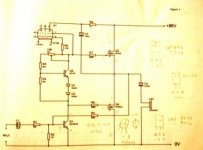
The single supply rail is +48V fullwave rectified voltage, giving mesured unloaded ~73V. The schematics is from EW 04 march issue by author Jeff Macaulay (sorry for the poor photo from the magazine). In his design the rail is +86V, and he is using 640/9640. Mine is estimated loaded voltage ~70V and I assumed that 540:s would be sufficient.
The cold tube will make a slow turnon, and as the pc88 heats up, the bias would bring on the Fets to the idle current adjusted earlier (~60-70mA)- that seemed to work ok. The saftey margin to Vs 20V should also be secured by the setting of the idle current prior to testing.
By the way- the to Fets (+100 -100) in my opinion would stand 200V in series, so the voltage margin should be even better. You say that the rail voltage could spike over the nominal voltage at power-up, how can that be? The maximum voltage available at all times cannot be more than 73V?
I always considered Fets to be rugged devices as they do not suffer by thermal runaway, but I might have to reconsider.
Regards Hans.
voltage spikes
Hans,
The mains voltage is subject to variations, I see +/-5% at my house all the time, my computers' UPS tells me it has 'protected' me from considerably more. With a normal, unregulated transformer based PSU, output will change in the same proportion as the input.
With respect to the output transistors being in series and therefore only seeing only half the rail voltage: This condition is only true for the idle condition. As soon as the output voltage moves one or the other of the transistors is dropping less of the voltage, the other is therefore seeing more. The limiting condition is at clipping where one transistor is completely on, seeing close to 0v, the other nearly off, subject to the entire rail voltage. Unfortunately, unlike power, you can't average device voltage, the transistor can (and will) 'break' in one cycle of audio.
All that having been said, your rail voltages are well within the rating of the FETs. Perhaps the next thing to check is the gate voltage, anything above ~20v will kill the FET very quickly. You might consider zeners to limit the voltage.
HTH
Stuart
Hans Olofsson said:Sorry, forgot to provide the schematics.
Hans.
As I suspected, this design does not limit gate-source voltage. It is VERY easy to fry a FET if the value is exceeded. In your case clipping is enough to do it. You URGENTLY need zeners in series with a diode (like 1N4148) to limit the gate-source voltage or you will fry any HEXFET you put in there eventually. It is possible this design was intended originally for laterals and was modified with a bias current servo. The laterals have built-in diodes.
Also, is your Q2 on the heatsink with the FETs? FYI, most MOSFETs do have a mechanism for thermal runaway (not as bad as bipolars though), the exception being lateral fets, which are really only 4 types in existance. Q2 and associated parts take care of bias current thermal stabilization, but Q2 needs to be on the heatsink.
Finally, I hate to burst your bubble but this is hardly an amplifier that makes any good use of a tube. Basically, it's working as a relatively poor current source, not much more than a glorified resistor. It's not amplifying or doing anything of the sort, sadly. If you removed the tube and put an appropriate resistor between the anode and cathode points, you would discover this amp works just fine (and probably not much different either). IMHO this is a waste of tubes. To make matters worse, it's not a very good construction regarding the rest of it either. There's the missing gate voltage limitig, already mentioned. And, I can't immagine that with no emitter degeneration in Q1, the DC point between the output FETs is stable at all (and it should be half the rail voltage for best results).
I apologize again for the poor photo- limited by the max file size of ~100k. The lower is 9540 and the upper 540 and the polarity should be correct. The Q2 is connected close to (i.e. right between the two Fets on a copper heat sink). All are of course electrically isolated from each other.
Yes, I realize that in working condition the voltage experienced by the transistors will in extremes be the full working voltage- but as mentioned earlier -73 is less than 100 which should suffice -a close margin but still a margin of at least 20V.
I agree with ilimzn -on second thought -that it seems to be a poor use of the pcc88, using it only as a current sink without any use of it as an amplifying device- pcc88 having a record of a excellent audio tube.
The destruction of the two Fets took place evidently instantaneously at the same time, so to me it seems that the destruction must have been caused by a bias overrun? (I have had this phenomena earlier -the destruction of the same 540/9540 without any reasonable cause).
If the lower Fet is saturating, the midpoint between the Fets should be close to zero and evidently the gate-to-drain voltage for the upper 540 might easily exceed 20V? Or do you have a suggestion to what might cause the the excess of 20V?
I took a look at the output on an oscilloscope and the square wave looked fine, the symmetry seemed fine (as far as I could see) but I noticed a definitive rounding of the wave, indicating a limited upper frequency- easily seen at 20 KHz. One of the 540:s nice properties is a very low Rds-on value of only 50 mOhms that should give an excellent damping factor- I'd be happy to keep them if possible.
So- you suggest adding a 15V? Zener in series with a 1N4148 connected between Gate and Drain? Any other suggestions?
The grid stopper value is 680 Ohms, should I increase them in order to protect the Zeners and would that detoriate the sound?
Thanks again- all your help is most valuable. A drawing would be helpful.
Regards Hans
no, gate to source protection.Hans Olofsson said:suggest adding a 15V? Zener in series with a 1N4148 connected between Gate and Drain?
the maximum is 15V.
look at the datasheet curves for Vgs vs Id. you may find the amp will deliver adequate current with 6V or 7V Zeners (+a diode). This also gives a bit of short circuit protection as well.
Hans Olofsson said:The destruction of the two Fets took place evidently instantaneously at the same time, so to me it seems that the destruction must have been caused by a bias overrun? (I have had this phenomena earlier -the destruction of the same 540/9540 without any reasonable cause).
Actually, that is unlikely - although it is possible, MOSFETs tend tu go into thermal runaway much slower than BJTs so you would have noticed the heatsing becoming very hot.
In the amp above, it is enough for sufficiently hard positive slipping to occur and the top MOSFET will be dead. This is because the PCC88 current source is bootstrapped from the output and can produce a higher voltage on the top MOSFET gate than the power supply voltage. The trick is that not much current is needed at all to damage the MOSFET gate insulation. Because the input stage of the amp can sompletely turn off with a sufficiently large input signal, you can exceed the absolute max Vgs of 20V on the top MOSFET, eventhrough the PCC88, if the peak is long enough.
In reality, what happens is that the insulation unlikely fails in one peak, but becomes progressively weaker. When it fails, MOSFETs have the regrettable tendency to fail short, which means the bottom MOSFET starts driving a short circuit to the power supply.
A short circuit to the output will also instantly kill the MOSFETs but not because of overcurrent, rather due to gate insulation destruction. This happens because with a short the output is fixed to mid voltage, and the input stage can still drive the full supply voltage to the MOSFETs - the input stage is only loaded by capacitive gates.
It should be obvious now why gate protection diodes are mandatory, like AndrewT said, even if they are not dimensioned to also provide a current limit. The actual MOSFET channel structure is far more rugged than the gate insulation.
One of the 540:s nice properties is a very low Rds-on value of only 50 mOhms that should give an excellent damping factor
Rdson has nothng to do with the damping factor, or indeed with the output impedance of the amplifier. It only shows you what the equivalent internal resistance of the MOSFET is when it is working in saturation mode (i.e. Vgs much more than needed for required current Id), in linear mode you never even get close to this as it would mean VERY hard overdriving the amp and clipping.
What does give you the low(ish) output impedance is the relatively hight Gm (also sometimes marked as S) of the HEXFET, although this also requires fairly bias (standing) current. The output impedance for class AB is roughly 1/Gm at the chosen bias current, and approaches 0.5/Gm as the bias current goes towards pure class A. Still, given thet Gm is only 5-10 A/V at rather high curents (several A!), the output impedance is only somewhat less than 1 ohm. This is however without global NFB applied, and in this amp there is global NFB. In any case, the output impedance will be sufficiently low, but not as low as with bipolar transistors on the output. But also, much lower than with lateral FETs at the output, because these have 5-10x less gm.
So- you suggest adding a 15V? Zener in series with a 1N4148 connected between Gate and Drain? Any other suggestions?
The grid stopper value is 680 Ohms, should I increase them in order to protect the Zeners and would that detoriate the sound?
No, as AndrewT said, gate to source. You can look up the Vgs versus Id plot for the transistors, and decide what the limiting voltage should be depending on the max. current you want to alow out of the MOSFETs. Mind that there are different curves for different temperatures, so you need to take care when reading the graph - especially if you are going into deep bias class AB - the transistors will be hot!
If your limiting voltage gets to be less than about 7V, you can omit the series 1N4148.
The reason for the series 1N4148 may not be readily apparent. They actually prevent the zener from acting as a regular diode in the oposite direction. Because the treshold voltage for these MOSFETs is about 3V, there will be about 6V difference between the gates of the lower and upper MOSFETs. When the output is fully driven, say positive, the gate of the lower MOSFET will move up in voltage as much as that of the upper MOSFET. If the G-S voltage across the upper voltage needs to become larger than 2x treshold voltage, a single zener diode on the oposite MOSFET would become forward biassed and would prevent the G-S voltage on the upper MOSFET becoming more than 2x treshold voltage + 0.6V, hence the limitiation to about 7V zeners if you want to use them with no series diodes to prevent this.
Regarding gate stoppers, no need to increase them. In fact, you may even decrease them as they play theri part in limiting HF response. Zeners can cope with rather large currents (especially if you use the 1W or 1.W variety) in peaks so you should not have a problem there. In general, if something fails as a result of really hard and long clipping (certainly minutes long), it is likely to be the resistors.
Lumba Ogir said:Hi,
Most importantly, you should use the tube as input stage taking advantage of its vast superiority for voltage amplification.
This is true but only with extra qualifications. In particular, with tubes, the less load there is, the more linear they are. Best with CCS on the plate - but then drive capability is diminished and you need quite a bit of it to drive a solid state output - even if it's made with MOSFETs. This is where many hybrids fall flat on their face. The way to avoid this comes through the proper choice of tube topology, the proper choice of tube and the proper design of the solid state output stage. In particular you want high and flat input impedance, which often means a much more complicated SS part than one would expect. Alternatively, if you want simplistic designs to drive SS well, you tend to end up using low gain low Rp tubes, which often means you need a good preamp.
Another thing that makes tubes potentially superior is that for the usual signals one uses in direct coupled amps, one actually uses only a small part of the full swing the tube stage is capable of. In most cases this means AC coupling the tube and SS stage. This is not as bad as it seems, but needs careful attention, there are pitfalls, especially if a feedbak loop is involved. On the other hand, there are DC coupled topologies that one can make a hybrid with, but these are by far not simple, and they place some restrictions on the tubes you can use too.
hmm yeah.. Zeners or something similar but no zener is going to fully protect from transistors internal oscillation if that happens, even it sounds ok you need to look at the signal in a scope..
In my humble opinion irf540&640 sucks...
Hmm I've had better results with irfp9140/240 (or higher depending on rail voltage)
You might want to look into the possability of using a tube with a hybrid mu-follower or something..
http://www7.taosnet.com/f10/figure3-4.gif like the rightmost variant with the fet.. irf810 or something like that..
hmm also I suspect thermal runaway,män dää gå ju att löösa..
Upupa Epops said:I don't understand, why you are talking about this schematic - there is all wrong and I mean, that author's knowledges about desigh of amps are near zero, which I tell diplomatically...
Well, that's more or less what I said, but more diplomatically
nikwal said:hmm yeah.. Zeners or something similar but no zener is going to fully protect from transistors internal oscillation if that happens, even it sounds ok you need to look at the signal in a scope..
Yes, and a high BW one, too. MOSFETs are known to be capable of >50MHz (often a lot more) oscilation or just ringing, and scopes with <100MHz bandwidth may not show that at all. The trick is keeping the inductance in the source line to a minimum, and gate buildout resistors to swamp out any negative input impedance phenomena.
In my humble opinion irf540&640 sucks...
Hmm I've had better results with irfp9140/240 (or higher depending on rail voltage)
Well, i wouldn't say that they actually SUCK, it's more of a problem that there are dozens of variants and manufacturers that are all supposedly the same - but they are not. Besides, if you really must use two from that series, make it IRF640 and IRF9540, both without any suffix at the end. IRFP9140/240 are also my favorites (I've been talking about them here for years
). Unfortunately, they are now also obsolete, the parts with an N suffix are not even nearly complementary (and I think IR does not make an IRFP9140N).Of course, one could always try Toshiba's J201/K1531 with a minor change to the bias generator, but that could get expensive.
- Status
- This old topic is closed. If you want to reopen this topic, contact a moderator using the "Report Post" button.
- Home
- Amplifiers
- Solid State
- On IRF540/9540