Upupa Epops said:I don't understand, why you are talking about this schematic - there is all wrong and I mean, that author's knowledges about desigh of amps are near zero, which I tell diplomatically...
Well, it's not exactly crash hot, but with a few simple mods it could still be turned into a not too shabby performer.
This is what I would do:
1) Pull that twin triode from its current silly location, along with the bootstrapping components and replace with a 5mA BJT current source, biased with a LED or a couple of 1N4148's in series.
2) Emitter degenerate the voltage amplifier transistor Q1 with a ~200 ohm resistor. This resistor will raise the emitter of Q1 to +1V (200R*5mA), thus making the DC bias stability adequate.
3) Connect a MPSA42 or similar as an emitter follower to drive Q1. Tie its collector to the positive rail and return its emitter to ground with a 1k8 resistor for a collector current of about 1mA. This emitter follower will reduce distortion caused by feedback via Q1's cob and non-linear base current through the input resistor.
4) Add a complementary emitter follower buffer stage between the Vbe multiplier and the MOSFETS. This design only has a single stage for voltage gain, so we want to keep the collector impedance of Q1 nice and high.
5) Add zener+diode gate protection for the MOSFETs as described already.
6) Tweak R2 to appropriately set the output voltage at approximately 1/2 the supply rail.
7) Add some freaking frequency compensation around Q1 in the simple form of a miller compensation capacitor from collector to the base of the added emitter follower (junction of R1,R2 and R3).
8) Shunt the Vbe multiplier with a ~10uF electrolytic.
9) If you really want to keep the valve in circuit, configure one half of the twin triode as common cathode preamplifier, with the other half as a direct coupled cathode follower to buffer the anode load of the other half from the input resistor R1. Maybe even use the cathode follower to bootstrap the anode load of the common cathode amplifier and set the preamp gain with the same type of NFB arrangement as used for the solid state part.
I think that’s about it
Cheers,
Glen
nitrate said:Hi,
Don't know if this helps but i've been using IRF640's in my classD creations and i've had nothing but trouble with them. They have always had a tendency to blow and go short accross all pins just for a laugh, Usally at power up. I'm convinced its a fault of the fets as the design seems to under run the fets by a long way. Can't imagine any reason why they should fail so often.... there dosnt seem to be any transients or over voltages to cause failures. Strange...........
Mad.P
undercharged bootstrap cap?
I studied the datasheet of the IR manufacture of 540/9540 and as I newer in this amp and in my situation ever will make use of the vast current available, a zener of ~5.5V/30A would make it?
I take no offence regarding the qualities of this design, but maybe Jeff M will (if he would come across these pages). As far as I understand he seems to have some reputation although...
The (short) time I had a chance to listen to it, I had no considerations regarding its musical qualities except maybe the limitations in higher frequencies. But I don't pretend to have golden ears.
On Fets as amplifying devices for those interested you might read http://sound.westhost.com/articles/hexfet.htm.
The author seems to advocate the use of heavy idle currents and expresses doubts on Fets as linear amplifiers as a whole.
Hans
Upupa Epops said:Wake up, Glen, sixtee's are fourty years away...
Ermmm....I didn't say that I would build it. I just made it reasonably OK, without too much extra complication, IMO.
Cheers,
Glen
My records on hybrid amps are not too fruitful:
I also tried a design of Generoso Cozza http://digilander.libero.it/essentialaudio/hybrid_circuit.htm and was unable to bring it up to full working voltage: +- 35V ( I used a variac) before it made a violent short, almost melting the 540/9540 in seconds and frying the .33 Ohm resistors. This design also lacks the Gate to Source zener protection. Apart from a flunked setup (I carefully checked for errors) would you say that the short at that time also was caused by the absence of GS protection?
The design seems to have an origin by Ernesto Borberly who claims it to be more or less a theft. http://www.tubecad.com/2004/blog0001.htm
Needless to say I abandoned the project when I failed to make it work.
Regards to you all for all input, I will implement the GS protection.
Hans
Hans,
how important is this project for you? Tubes should be taken for what they are and not be used like solid state devices. Low anode voltages just mean high distortion and bad sound. Furthermore triodes "do not like" low anode impedances. An active CCS of some kind will greatly improve linearity. Why not a small signal penthode? That combination would give you unbeatable sound quality and driving ability. I am proposing separate high voltage B+ and AC coupling because to me, it is the only meaningful way to go for a hybrid amplifier.
how important is this project for you? Tubes should be taken for what they are and not be used like solid state devices. Low anode voltages just mean high distortion and bad sound. Furthermore triodes "do not like" low anode impedances. An active CCS of some kind will greatly improve linearity. Why not a small signal penthode? That combination would give you unbeatable sound quality and driving ability. I am proposing separate high voltage B+ and AC coupling because to me, it is the only meaningful way to go for a hybrid amplifier.
Hans Olofsson said:My records on hybrid amps are not too fruitful:
I also tried a design of Generoso Cozza http://digilander.libero.it/essentialaudio/hybrid_circuit.htm and was unable to bring it up to full working voltage: +- 35V ( I used a variac) before it made a violent short, almost melting the 540/9540 in seconds and frying the .33 Ohm resistors. This design also lacks the Gate to Source zener protection. Apart from a flunked setup (I carefully checked for errors) would you say that the short at that time also was caused by the absence of GS protection?
Probably the root cause is oscillation, which will sometimes fry MOSFETs even with gate protection, but certainly when they are without it.
This design does work, but requires careful attention to routing and some parts selections. It alsio requires ner to perfect thermal management of the MOSFETs as it is a class A amplifier - with realistic mounting techniques and heatsinks, the IRF parts will be at the very limit of endurance.
Also, the PCC/ECC88 was designed to work at VHF, closing in to UHF frequencies, and without proper management (routing, grid stoppers...), it likes to oscillate on it's own at hundreds of MHz. In fact, it is often said that in most cases where sub-par sound quality is claimed for this tube, the underlying problem is oscillation.
On both account i can speak from personal experience.
As Lumba Ogir said, the design has other flaws, one of them being the low voltage across the tube, which even for a 6DJ8 family tube is very low. Perhaps an ECC86 would work better here but even that would require some changes. The basic topology can, however, be improved to give the tube a better operating conditions
All in all, it is on the surface a simple design but it has many hidden pitfalls. You ight want to try making it into a headphone amp for starters, by increasing the 0.33 ohm resistors and thus lowering the bias current of the output stage. It should be noted that using inductive parts (wirewound...) in these positions is asking for trouble! Such a headphone amp could then be used as a driver for a follower stage (with MOSFETs or BJTs) and form a much less crytical power amp. The advantage being, you could take the design in stages.
Also, like Lumba Ogir said, AC coupling is the most viable option, vecause it alowes you to have completely separate power supplies for the tube and SS stages, and so optimize them for their particular role. Another, perhaps not so obvious plus of this approcah, is that you can again take your project in stages - make a tube stage and test it, make a SS stage and test it, then connect them together, and then, as a fourth step, perhaps provide a feedback loop or some similar extra functionality. There will sometimes be a restriction that this sort of amplifier will have no global NFB, which is not necesairly a problem ith the tube part, but can be with the SS part, requiring very low distortion running open loop.
As for using a pentode for the front end, although I am sure this approach will find controversy and objections from many in these forums, I personally am all for it. Some extremely common and cheap pentodes can be set up simply for rather amazing performance - like >100x gain, at less than 1% well behaved THD for over 100V of output swing. Some of these have sufficient gm that appreciable current can be sourced without compromising the other parameters. Those parameters can also be further improved by adding local NFB around the tube stage to lower gain to that more commonly found in power amps, or, with the right care and attention, a global NFB loop could be used. The tubes to look at would be high gm pentodes for IF and RF service as well as so called video pentodes, that were used to drive CRTs.
Lumba, the project is really not very important, but I am trying to find out why the designs seem to blow up in my face- it is obvious that many of the published amp projects have flaws.
I made my own PCB for the Cozza amp -a tidy setup in my own opinion- however- I could not say whether it was safe regarding the VHF/UHF issue. I know that the PCC88 was used in older TV sets as UHF amplifying devices but many sources say it is an excellent audio tube due to the low working voltage and low internal impedance. Would not the 100 Ohm grid stopper prevent the FETs to oscillate? The FETs were all heavily heatsinked.
You mention IF/RF pentodes- I have loads of good EF80, PCF80 and likes, collected out of garbage TV sets, any suitable for audio use? - the "F" indicates low power pentodes.
Hans
Hans,
my previous post was a kind of misunderstanding (happens often to me), I was suggesting an input topology for the other design, still having that in mind, very confusing, I am sorry.
Now we are talking about this amplifier, right, here is another link:
http://digilander.libero.it/essentialaudio/hybrid_main_power_amplifier_+sche.htm
It should be important to get it working. Borbely made a line amp based on the topology but a very similar power amp was published in TAA or GA. I am not able to find the article. Now, everything looks fine to me, the constant current arrangement is scant, maybe OK. It simply has to work. Check your soldering.
PCC88 is a widely used and preferred type, there is absolutely nothing wrong with it. The problem must lie elsewhere. Did you test the input stage separately? Did you initially use higher values of source resistors?
Source resistors need to be non-inductive.
PCC88/ECC88 are the same thing with a (slightly) different heater. Be sure to use grid stopper resistors with this tube as it likes to oscillate if you don't.
As Lumba says, there is nothing inherently wrong with the topology, but some bits could be improved. The current source on the output, for instance. Because MOSFETs have relatively high tolerances on Vgs, and it's also temperature dependant, you might waht to use a 'ring of two' CCS instead (BJT monitors voltage on source resistor of the MOSFET by it's B-E being connected across it, and 'takes away' the gate drive of the MOSFET via it's collector).
Regarding EF80 and PCF80, both are eminently usable (if not popular) for audio.
EF80 can work very linear as a pentode stage, and also makes a prety good triode. The only problem is that there are many versions around as it was used literally by the million in TV and radio sets, and it was not specified originally to be particulairly non-microphonic, so there are versions out there that can be a problem in that regard - but then, there are also very good ones. In fact, EF80 could be used pentode connected as a tube stage for a hybrid amp, where the SS stage is a buffer (has a voltage gain of <=1).
ECF80 was used in several very well known european tube amps, normally the pentode as input stage, and triode as concertina phase splitter. The triode part at first glance seems similar to half of an ECC82, but it is more linear and better in several key parameters, although being in a shared envelope, capable of less heat dissipation. The pentode works fine, and makes a good triode, too. PCF80 has a different heater, but unlike the PCC/ECC88 the difference is quite large (if i remember right, it's a 9V/300mA heater), which makes the tube unpopular - you should use this fact as it is widely available and cheap. The same caveat applies re microphony as with the EF80.
Well, Lumba - I used the component values suggested, no changes. As I remember (I abandoned the project some years ago) I failed to make the input stage work properly and after the blowing of the FETs I connected two power resistors (10 Ohms) in series with the + and - supply terminals with the + and - inputs to the board. The idea was to protect the power devices and burn the resistors first. Most confusingly that made no difference at all-still blowing the FETs most violently! At that stage I gave up in total bewilderment.
I remember suggesting like ilimzn, high frequency oscillation but still, RF draws current and the resistors should have protected the devices anyway.
ilimzn- please explain more specificly Because MOSFETs have relatively high tolerances on Vgs, and it's also temperature dependant, you might want to use a 'ring of two' CCS instead (BJT monitors voltage on source resistor of the MOSFET by it's B-E being connected across it, and 'takes away' the gate drive of the MOSFET via it's collector)
Thanks Hans
Hans Olofsson said:ilimzn- please explain more specificly Because MOSFETs have relatively high tolerances on Vgs, and it's also temperature dependant, you might want to use a 'ring of two' CCS instead (BJT monitors voltage on source resistor of the MOSFET by it's B-E being connected across it, and 'takes away' the gate drive of the MOSFET via it's collector)
Thanks Hans [/B]
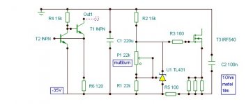
The original schematic relies on Vgs of the lower output MOSFET to set the CCS current. It is basically the voltage on the gate of this MOSFET, minus Vgs required for this CCS current, divided by the source resistor of the MOSFET. The problem here is that while the voltage on the gate can be made well defined (by a zener, diode string, etc), the Vgs of the MOSFET depends on the particular MOSFET itself - not only the particular type used, but also within the same type there can be large tolerances, especially for the same type from different manufacturers, and on the temperature of the MOSFET. Therefore, without some sort of an adjustment and thermal compensation, this CCS current is not well defined.
This is why a different type of CCS needs to be put in that position. Instead of relying on several variables, you can reduce this to only one, by constructing a CCS which tries to maintain one Vbe voltage drop of a BJT on the source resistor of the MOSFET. Then the current is only dependant on the Vbe change with temperature of the BJT, and the current through the collector of the BJT, which can be stabilized the same way as the gate voltage in the original version of the CCS was stabilised (in fact, you can use this same 'voltage reference' for the input stage differential CCS, saving a part or two).
In general, this is how you do it:
First provide a voltage reference off the V0 rail. You do this by tying a suitable zener in series with a resistor from -V to GND. The zener anode goes to -V. The zener cathode is the reference p[oint.
Next, connect a resistor much larger than the series zener resistor, from the reference point to the gate of the bottom MOSFET (N-ch). The source of this MOSFET remains connected to -V through a source resistor, as it is now.
Then, connect a NPN BJT so that it's collector goes to the MOSFET gate, it's base to the MOSFET source, and it's emitter to V-. This puts the B-E junction directly across the MOSFET source resistor.
The resistor from thereference point supplies positive gate voltage to turn on the MOSFET. However, if the voltage across the source resistor rises as a result, the BJT starts conducting and shunts the MOSFET gate voltage to V-, therefore limiting it so that the current through the source resistor creates a voltage drop equal to about 0.55-0.6V for typical small signal BJTs. In other words, it's anegative feedback based CCS.
The advantage of this CCS is that a relatively small voltage drop is needed on the source resistor, and the Vbe of the BJT changes by about 2-3mV/degC so assuming a relatively constant reference, this is the only source of CCS current change. In actuality, the BJT can be kept sufficiently away from the MOSFET to reduce temperature dependancy, but even with 50deg C difference between hot and cold, the tolerance of the CCS will be +-10%, which is far better than that of the original. With the original, the drop on the source resistor has to be quite large compared to the Vgs of the MOSFET to keep the Vgs variations small in comparison - so, a lot of voltage (and heat) is lost across the source resistor.
Thanks both of you.
In my mind these concepts works as a servo controlling the DC current through the transistors. The interesting question now- can this now be applied to an AC condition ? Would not the servo cancel all AC components applied to the gate of the transistor? That is- is this something to be added to the existing circuit?
Hans
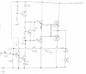
Attachments
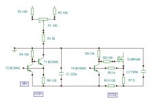
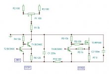
Hi Hans,
these are constant current sources, just like those in the original circuit. (D1, P3, R5, R15, Q3)
The base-emitter voltage of T2 and T4 are utilized as reference voltages instead of the zener diode.
The current of the input stage will be: 0.6V/R6=5mA, in the output stage: 0,6V/R7
Omit D1, P3, R5, R15 and break the connection towards R11.
Attachments
- Status
- This old topic is closed. If you want to reopen this topic, contact a moderator using the "Report Post" button.
- Home
- Amplifiers
- Solid State
- On IRF540/9540