I'm coming to this thread late mainly by searching for sliding bias topology. So my assumption is that this reworking of the original Mullard amp (brilliant work Lumanaw, LXG & Nordic) has retained this sliding bias topology!
I see this hasn't had activity since 7/2008 - has nobody built this? It looked to have so much potential!
What is the dissipation of the O/P devices - is it operating at a lower bias than full class A as is possible with sliding bias?
I hope there is a good outcome to this post as it seems a shame to let this one die!
Thanks - no, it's not dead by a long shot. There are two prototype PCB layouts on this thread, both started by Nordic. I was hoping somebody would take it from there, make a prototype and see how it sounded.
The dissipation depends on the rail voltage(s) and the quiescent current - at +/- 24V and 1.25 A, it's 60W dissipation per ch., but you can safely lower the rail voltages to as low as +/- 12 V, Icq=1A for approx. 6W per ch. output power into 8 ohms., with a dissipation of 24W/ch, Class-AB at max swings.
The dissipation depends on the rail voltage(s) and the quiescent current - at +/- 24V and 1.25 A, it's 60W dissipation per ch., but you can safely lower the rail voltages to as low as +/- 12 V, Icq=1A for approx. 6W per ch. output power into 8 ohms., with a dissipation of 24W/ch, Class-AB at max swings.
Thanks LXG,
Are these not class-A dissipation ranges? What does the sliding bias do?
With those sort of exemplary THD figures the only question is how does it sound - you built some early prototypes, I think - what were your impressions?
Nordic, how did the prototype from the pics work out? And same question to you.
A very old Schematic of Mullard Amp
Dear all,
As I was browing the various threads, I stumbled on this thread and read it completely. I made notes on a paper about 40 years back and also copied the drawing. I copied the drawing into LTspice and my notes, what ever I could retrieve are as below. Hope this will be of interest!
I used to be very careful in making notes, but in this drawing, the circuit around Tr2 & 3 and Feed back is not clear to me. Please I want to understand the operation of this circuit as an exercise. Can any body who followed the scheme explain it a bit and show how the Power dissipation etc are derived?
Provided the load does not at any frequency fall below Rl = Vc/(Pi*Iq), crossover distortion cannot appear. With this particular method of class AB, (Pi mode AB), the collector dissipation is maximum under no drive conditions and Pc = Vc*Icpk/Pi which is nearly equal to 2/3 Pout (Max)
---------------------------------------------
The changeover from Class A to class AB operation occurs at 0.4*Pout max.
Overall Negative Feed Back of 44db is applied.
The Stability of the collector currents is ensured by direct coupling the phase splitter to the output stage and by over all negative DC feed back. Thus Iq through output transisters is defined by one Nfb loop and midpoint voltage by the other loop.
The normal collector dissipation of the output Transister = 9.2 watts/trans
Max Pc = (+30%) = 12.2 watts.
If Iq is reduced to 0.27 amps, 5 watts output for constant Sine wave drive.
Max dissipation = 8.3 watts.
Dissipation of OC 81 Z = 500 mw.
Dissipation of TR3 = 160 mw.
If the emitter Resistance, decoupled, is made large enough so that the DC is well defined, then the dynamic Bias condition of the transistor has to adjust itself with drive so as to maintain constant DC. Upto a certain power level, both the transistors operate in class A PP. Beyound this point, each transistor is cut off for part of the cycle. Also each transistor sees half the class A load during that part of the cycle during which its partner is cut off. As the drive is increased beyond this point, the total current will also tend to increase. The operating point will however shift so as to return the overall DC consumption to its previous value. With the increasing drive, the operation shifts to class B and then to class C conditions.
For audio amp applications, the design shold be such that the class B condition is reached at max power output. For this case, the Iq, Ipk, Vc & Rl are related by
Iq = Ipk/Pi = Vc/piRl, where Ipk is the peak current at max output, and Rl is the load seen by each collector independently. The design of the output stages is the same as for a Class B stage, delivering the same power but the ---
------------------------------
Dear all,
As I was browing the various threads, I stumbled on this thread and read it completely. I made notes on a paper about 40 years back and also copied the drawing. I copied the drawing into LTspice and my notes, what ever I could retrieve are as below. Hope this will be of interest!
I used to be very careful in making notes, but in this drawing, the circuit around Tr2 & 3 and Feed back is not clear to me. Please I want to understand the operation of this circuit as an exercise. Can any body who followed the scheme explain it a bit and show how the Power dissipation etc are derived?
Mullard 10 watt amplifier.
Normal Loading, Iq = 0.4 amps.
Low Loading, Iq = 0.27 amps.
Ripple < 100 mv.
Iq = Ipk/Pi and Pout = Icpk*Vcpk/2Normal Loading, Iq = 0.4 amps.
Low Loading, Iq = 0.27 amps.
Ripple < 100 mv.
Provided the load does not at any frequency fall below Rl = Vc/(Pi*Iq), crossover distortion cannot appear. With this particular method of class AB, (Pi mode AB), the collector dissipation is maximum under no drive conditions and Pc = Vc*Icpk/Pi which is nearly equal to 2/3 Pout (Max)
---------------------------------------------
The changeover from Class A to class AB operation occurs at 0.4*Pout max.
Overall Negative Feed Back of 44db is applied.
The Stability of the collector currents is ensured by direct coupling the phase splitter to the output stage and by over all negative DC feed back. Thus Iq through output transisters is defined by one Nfb loop and midpoint voltage by the other loop.
The normal collector dissipation of the output Transister = 9.2 watts/trans
Max Pc = (+30%) = 12.2 watts.
If Iq is reduced to 0.27 amps, 5 watts output for constant Sine wave drive.
Max dissipation = 8.3 watts.
Dissipation of OC 81 Z = 500 mw.
Dissipation of TR3 = 160 mw.
If the emitter Resistance, decoupled, is made large enough so that the DC is well defined, then the dynamic Bias condition of the transistor has to adjust itself with drive so as to maintain constant DC. Upto a certain power level, both the transistors operate in class A PP. Beyound this point, each transistor is cut off for part of the cycle. Also each transistor sees half the class A load during that part of the cycle during which its partner is cut off. As the drive is increased beyond this point, the total current will also tend to increase. The operating point will however shift so as to return the overall DC consumption to its previous value. With the increasing drive, the operation shifts to class B and then to class C conditions.
For audio amp applications, the design shold be such that the class B condition is reached at max power output. For this case, the Iq, Ipk, Vc & Rl are related by
Iq = Ipk/Pi = Vc/piRl, where Ipk is the peak current at max output, and Rl is the load seen by each collector independently. The design of the output stages is the same as for a Class B stage, delivering the same power but the ---
------------------------------
Attachments
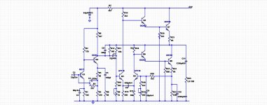
I used to be very careful in making notes, but in this drawing, the circuit around Tr2 & 3 and Feed back is not clear to me. Please I want to understand the operation of this circuit as an exercise. Can any body who followed the scheme explain it a bit and show how the Power dissipation etc are derived?
I missed this posting earlier - thanks for your schematic. Yes, it's one of the Mullard sliding-bias circuits, and notable for the use of only PNP transistors (in the germanium era, PNPs were the more common transistors).
I decided to revisit this topology after being inspired by the Amp Camp Amp. In particular, the use of +/- 19V supplies derived from laptop AC adapters seems to be viable. I do have an updated schematic with DMOS output devices, which I'll post in due course - there's also a PCB layout in progress.
Hi
The input stage operate as current feedback units, not like standard voltage feedback that is generally used now. Q1 derives feedback from the emitter of Q2, and should be fed with a current (high impedance) source ideally. Q2 then has its emitter voltage controlled by feedback, so this point is low impedance, but the current is taken from the collector, so this is a high impedance output (current fed) output.
The feedback resistor R12 in the output stage then converts the input current to voltage output.
The starting bias conditions can be calculated by guesstimating that the output rail will be approximately the same as the collector voltage of Q3 (you could also assume 0.7V lower from two Vbe's and the drop across R23 at 0.3A). So then we have for Q3
Vb~ R/(R+18k)*Vc (or Vc-0.7)
where R=2.2k plus mid-pot 500 ohms (as a starting point)
Ve=Vb-0.2 (approx)
Ic=Ve/560 (approx)
Vc=Vcc-3.3k*Ic
Vc=Vcc-3300/560*Ve
Let A=2.7k/(2.7k+18k)
then
Vb=A(Vcc-3300/560*Ve)
Vb=A(Vcc-3300/560*(Vb-0.2))
which after a shuffle gives
Vb=4.5
so this would suggest that the centre rail does operate about half the supply. It should be a bit higher to allow for the voltage drop in the lower part of the circuit, perhaps around (-)28V.
To conduct the same current the lower half controlled by Q4 will conduct approx. the same current in the collector setting the voltage across R22 to about 4.5V, setting Iq to about 300mA. Detailed calculations can be done as above (there is no DC link between Q3 and Q4 so these can be solved separately).
This circuit may have been novel at the time but Q3 operates with a swinging collector while Q4 will remain relatively low, so there is an imbalance between the halves of the circuit and Early effect distortion will be rather high.
With approx. 300mA bias current in idling, the power dissipation will be approx. 7W per output transistor. One problem with such circuits is that if the DC bias point changes, there will be a DC ripple effect through the circuit which will change again when the signal reduces again, causing spurious low frequency currents arising in the output.
The frequency performance of Ge transistors was not great, either, so not much positive to say about this as a hifi- more of historical interest.
John
Member
Joined 2009
Paid Member
Dear all,
As I was browing the various threads, I stumbled on this thread and read it completely. I made notes on a paper about 40 years back and also copied the drawing. I copied the drawing into LTspice and my notes, what ever I could retrieve are as below.
The input stage, Q1 and Q2, looks to me as if it was designed by a person who really wanted to make a CFP/Sziklai but didn't have any NPN devices - so concocted a way to make a feedback pair out of two PNP's. I wouldn't do this nowadays.
Anybody notice the similarities between this sliding bias scheme and the one that Elvee publishes as his circlophone?
The frequency performance of Ge transistors was not great, either, so not much positive to say about this as a hifi- more of historical interest.
plenty of folk built radios with Ge transistors - plenty enough for small-signal hi-if and perhaps there are power Ge devices fast enough too ?
Last edited:
The input stage, Q1 and Q2, looks to me as if it was designed by a person who really wanted to make a CFP/Sziklai but didn't have any NPN devices - so concocted a way to make a feedback pair out of two PNP's. I wouldn't do this nowadays.
The Mullard sliding-bias designs from P. Thama (?) date back to about 1960, almost the dawn of the solid-state era. At the time, the only devices available easily were some Germanium PNPs. Some later versions of the same designs use an NPN input (when they became available), and even later versions like the 1976 Elektor version use mostly NPN silicon commodity parts.
(Today, I'd use Japanese small signal NPNs like the 2sc1845, and IRFP150 or similar for the outputs. Also compare with the AmpCamp Amp - the Mullard is competitive.)
...perhaps there are power Ge devices fast enough too ?
Power Ge devices, yes. Fast enough - depends on what's considered fast:
AD149 - TO3, 3.5A, 50V, 500 kHz. They used to blow up at the slightest sign of thermal runaway on a hot summer's day. I still have a few left over, made by Bharat Electronics (BEL) well into the early-'80s.
Is there a simple solution to tackle the turn-on thump? Massive, jumps to about 4V and back to zero. Quite audible and though not an issue for the cheap little test speaker, I had built this to test higher efficiency speakers. Not so sure it is a good idea to push that much DC into delicate little coils. A delay is a good solution, but was fishing for others.
I built the last layout Bigun (thanks, man!) had posted, and promptly burnt through an entire batch of BC547/557 because I religiously followed the layout forgetting to reverse the devices. Fortunately the outputs were all right.
The input is highly sensitive to RF. Sounds good but no measurements yet.
I am using a very tiny heatsink with sloppily mounted outputs and I have a fan blowing over it, the MOSFETs run really hot and I burnt my finger while testing for temperature (so let's say about 80C). The sinks run just warm to the touch because of the fan. Running of a pair of laptop supplies with a CRC filter to help a bit with the HF noise. Not that there's much of it, but that will be proved or not in the days to come when I run it with 94dB+ speakers.
The ACA is also on my radar for the exact same purpose and 5 watts seems to just perfect. Plus, I already have the supplies
I built the last layout Bigun (thanks, man!) had posted,
I meant Nordic, of course
Anyone else got prototypes running?
Is there a simple solution to tackle the turn-on thump? Massive, jumps to about 4V and back to zero. Quite audible and though not an issue for the cheap little test speaker, I had built this to test higher efficiency speakers. Not so sure it is a good idea to push that much DC into delicate little coils. A delay is a good solution, but was fishing for others.
...
The input is highly sensitive to RF. Sounds good but no measurements yet.
Cool - so it almost does work, then
Turn-on thump: I obviously missed that in simulation, but it's likely to be present in most sliding-bias designs in some form - there's a large cap at the output that needs to be charged before the biasing stabilizes. A relay-based speaker-protect seems to be required.
RF: That can be fixed by tweaking the input RC filter - change to something with a 0.7 usec time constant. 3k3 and 220pF are common choices.
Laptop supplies: are you running +/- 19V into it? That's what I'm looking at too, though +/- 12V may keep the dissipation more manageable.
Hi
It is a great sounding amp, so thanks for the effort I was running +/-19V and full bias (worked out to 1A when measured across the 1E resistor). Using a pair of 80mm fans and chipamp-style sinks, temps were under 40 degrees C at all times because of the fans. Plenty of thermal headroom as of now.
I eventually had to use a delayed turn-on using a single PNP transistor and some relays, but even that was not enough to prevent the negative side laptop brick from destruction. Repeated charging of 20kuF plus another 10k on the CRC filter was enough to brick it. The primary side cap was blown, and the transformer badly overheated. I suspect the secondary side rectifier was also dead. Wasn't pretty. I was using 65W 3.5A bricks, but I suspect even the bigger ones would be marginally designed and am hesitant of investing more money in China's cottage industry. 19V rails works out to 13V swing/8W ch, which is right about where I need it to be.
I am considering other supply options to be able to eliminate both the 50Hz noise and allow enough overhead to charge the bias caps. I think it sounds a tiny bit better than the F5 I built earlier, and this is before you put in the folded current mirrors. Since speed was of the essence I used the layout posted earlier.
One more question: R16 and bias - inverse or direct relationship? I may use higher rails from transformers I have laying around, but will need to tune the bias downward. I may be looking at a custom SMPS design for this specific build. I want a portable Class A amp, so transformers are an issue.
RF: it isn't an issue when an input is connected only when there is no low-impedance termination at either end of the cable. Then putting your finger or a screwdriver within a few inches of the input has a loud hum coming through. I suspect the input layout does not properly account for the very high input impedance. Not an issue in practice though, and I can always kill it by hanging a 10k resistor off the input terminals to kill it.
Good things about the amp, apart from its sound, is that is is totally short-circuit proof (ask me how I know!) and absence of a rail does not kill the output, though is difficult for speakers to handle. Powering the protector off the two ends of the supply seem to take care of that completely.
It is a great sounding amp, so thanks for the effort
I was running +/-19V and full bias (worked out to 1A when measured across the 1E resistor). Using a pair of 80mm fans and chipamp-style sinks, temps were under 40 degrees C at all times because of the fans. Plenty of thermal headroom as of now.I eventually had to use a delayed turn-on using a single PNP transistor and some relays, but even that was not enough to prevent the negative side laptop brick from destruction. Repeated charging of 20kuF plus another 10k on the CRC filter was enough to brick it. The primary side cap was blown, and the transformer badly overheated. I suspect the secondary side rectifier was also dead. Wasn't pretty. I was using 65W 3.5A bricks, but I suspect even the bigger ones would be marginally designed and am hesitant of investing more money in China's cottage industry. 19V rails works out to 13V swing/8W ch, which is right about where I need it to be.
I am considering other supply options to be able to eliminate both the 50Hz noise and allow enough overhead to charge the bias caps. I think it sounds a tiny bit better than the F5 I built earlier, and this is before you put in the folded current mirrors. Since speed was of the essence I used the layout posted earlier.
One more question: R16 and bias - inverse or direct relationship? I may use higher rails from transformers I have laying around, but will need to tune the bias downward. I may be looking at a custom SMPS design for this specific build. I want a portable Class A amp, so transformers are an issue.
RF: it isn't an issue when an input is connected
only when there is no low-impedance termination at either end of the cable. Then putting your finger or a screwdriver within a few inches of the input has a loud hum coming through. I suspect the input layout does not properly account for the very high input impedance. Not an issue in practice though, and I can always kill it by hanging a 10k resistor off the input terminals to kill it.Good things about the amp, apart from its sound, is that is is totally short-circuit proof (ask me how I know!) and absence of a rail does not kill the output, though is difficult for speakers to handle. Powering the protector off the two ends of the supply seem to take care of that completely.
While we're asking questions, how do you plan to charge 20kuF of caps through SMPS?
The primary side of small laptop supplies have about 47uF of capacitance.
The negative side supply is under massive pressure when you push the amp hard. The repeated charge discharge cycles of the sliding bias cap basically killed the negative side supply - thankfully, only $5 worth. Am going to try again after I buy another, as I don't want a linear supply for this one as one of the ideas was to keep it handheld - a Clas A amp that you could carry on the Metro.
The surviving positive side supply has been fitted with a much nicer 100uF Hitachi cap. I am slightly more confident of the supply's ability, but we'll see when the rubber meets the road. I don't think there is still enough juice to properly power the amp. You need a supply capable of large short-term current peaks, which points one away from SMPS, or a change to the sliding bias arrangement/values. Smaller caps with the expected, smaller peak Class A capabilities?
While we're asking questions, how do you plan to charge 20kuF of caps through SMPS?
The primary side of small laptop supplies have about 47uF of capacitance.
The negative side supply is under massive pressure when you push the amp hard. The repeated charge discharge cycles of the sliding bias cap basically killed the negative side supply - thankfully, only $5 worth. Am going to try again after I buy another, as I don't want a linear supply for this one as one of the ideas was to keep it handheld - a Clas A amp that you could carry on the Metro.
You have 220V mains on the metro? or you just want to be able to lug it along?
I've used 2x 19V/2.1A netbook adapters with 47uF primary and 470uF secondary to power a Class-AB composite gainclone (MiniRef), which has 4700uF on each rail. It powers on without a thump, but there's a speaker-protect relay also in the setup. I think the netbook AC adapter can handle start-up transient capacitive loads up to 10,000uF on each rail, but still need to check the long-term reliability of such an arrangement (4700uF has been working for over a year).
However, I did upgrade all the secondary side capacitors in the adapters with Rubycon ZL/ZLG/ZLH, which have exceptional ripple current and durability for the size. The stress is mostly going to be limited to a fraction of a second during startup, when it will be at full duty cycle to charge the large caps.
The Metro is a conceptual expression
AB amps would not be an issue, I suspect, even with basic adapters.
But a combination of 2A constant bias and the 10kuF on the rail (stereo, 3.5A adapters here) is probably an order of magnitude worse.
I think primary side is stressed more under these conditions. Low ripple on secondary side is slightly easier to achieve than current delivery from primary. I know as much about SMPS as a farmer knows quantum mechanics, so I'll stop here.
I shall await your progress and report back at the end of the week, a sacrifice of $15 is probably going to be the order of the day but we'll see. I have a slightly better Coolermaster NA series adapter, but even that is 65W/and I'm keen to preserve it for other applications, hence will be using it for positive side supply.
- Status
- This old topic is closed. If you want to reopen this topic, contact a moderator using the "Report Post" button.
- Home
- Amplifiers
- Solid State
- Mullard SS power amplifier