Finally my boost converter is reaching an acceptable performance.
It gave some more headache to me than expected.
- ...tuning the regulation loop for stable operation at low power, while
providing proper THD....
- Reverse capacitance of the MosFets caused the PFC-chip to oscillate,
due to incredible turn OFF du/dt of Vds....
At 230V input it can continuosly deliver about 800W.
All temperatures a remaining below 70°C during this load.
Max. power is around 1kW.
But I am not so lucky with my snubber losses.
The CDR snubber (C:2n2 , D: BYT08P1000, R:500 Ohms) looks
nice in schematic and is working fine in reality, but the losses.
...especially at low power loads...
...at 200kHz this snubber will make losses of
P=200kHz x 0.5 x 2.2nF x (470V)^2 = 49W.

I already tried some variations.
- smaller snubber cap:
Well, high du/dt causes two drawbacks. EMI issues and additional ir
directly can disturbe the PFC chip itself. In the beginning I was working with du/dt up to 30kV/us.... Don't ask ! My radio made more noise than music, laptop ignored its touch pad....
This happens only at high loads, because then the current in the MosFets goes up to 12A and these 12A are forcing the sloping speed of Vds during MosFet turn OFF.
The reverse capacity of the MosFets is demanding quite a low driving impedance to and I had to implement the five BC560 to drive and decouple these beasts from the PFC chip.
The snubber with 2.2nF now limits the sloping speed to about 5kV/us. Which is fine for proper operation and also for my radio and all other stuff I am using here...
I also tried to reduce the switching speed and save the snubber, because the MosFets could easily handle some turn OFF losses.
a) ..by a higher driving impedance, but I got some turn OFF oscillation around 10MHz.
b) ..by a well damped RC-feedback from drain to gate, also this
resulted in inconvinient turn OFF oscillations at high power load.
OK, I hoped that I could at least use some of the snubber energy for the chip supply... , well the snubber pulses caused some irritations to the chip and the detect signal was not detected proper anymore....
Hm, now I am thinking about some resonant "lossless" snubber, but
my brain did not come up with a proper idea up to now....
(...typically running into demag issues already in theory.)

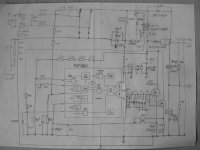
Good ideas are welcome. Sorry for the poor quality of attached schematic.
It gave some more headache to me than expected.
- ...tuning the regulation loop for stable operation at low power, while
providing proper THD....
- Reverse capacitance of the MosFets caused the PFC-chip to oscillate,
due to incredible turn OFF du/dt of Vds....
At 230V input it can continuosly deliver about 800W.
All temperatures a remaining below 70°C during this load.
Max. power is around 1kW.
But I am not so lucky with my snubber losses.
The CDR snubber (C:2n2 , D: BYT08P1000, R:500 Ohms) looks
nice in schematic and is working fine in reality, but the losses.
...especially at low power loads...
...at 200kHz this snubber will make losses of
P=200kHz x 0.5 x 2.2nF x (470V)^2 = 49W.
I already tried some variations.
- smaller snubber cap:
Well, high du/dt causes two drawbacks. EMI issues and additional ir
directly can disturbe the PFC chip itself. In the beginning I was working with du/dt up to 30kV/us.... Don't ask ! My radio made more noise than music, laptop ignored its touch pad....
This happens only at high loads, because then the current in the MosFets goes up to 12A and these 12A are forcing the sloping speed of Vds during MosFet turn OFF.
The reverse capacity of the MosFets is demanding quite a low driving impedance to and I had to implement the five BC560 to drive and decouple these beasts from the PFC chip.
The snubber with 2.2nF now limits the sloping speed to about 5kV/us. Which is fine for proper operation and also for my radio and all other stuff I am using here...
I also tried to reduce the switching speed and save the snubber, because the MosFets could easily handle some turn OFF losses.
a) ..by a higher driving impedance, but I got some turn OFF oscillation around 10MHz.
b) ..by a well damped RC-feedback from drain to gate, also this
resulted in inconvinient turn OFF oscillations at high power load.
OK, I hoped that I could at least use some of the snubber energy for the chip supply... , well the snubber pulses caused some irritations to the chip and the detect signal was not detected proper anymore....
Hm, now I am thinking about some resonant "lossless" snubber, but
my brain did not come up with a proper idea up to now....
(...typically running into demag issues already in theory.)
Good ideas are welcome. Sorry for the poor quality of attached schematic.
Attachments
mzzj said:30kV/us, sounds scary. I am sure that all Hams around you have been mad as hell during your tests
...hams: I am afraid you are right.
Also some kids with RC cars might have had some headache.

30Kv/us slopes?
For a 400V output that would imply a 13ns rise time. I dont remember what MOSFETs are you using, but I think that it's quite hard to go below 50ns due to output and reverse transfer capacitances.
Also, such a rise time would generate a huge voltage spike due to leakage inductances and due to the fact that diodes take several dozens of nanoseconds to start showing a low impedance.
Furthermore, that voltage-rise spike would be coupled to the other side of the boost inductor due to winding capacitance and will be very hard to filter. At these frequencies everything is just an antenna. In comparison, a piece of 10Mhz ringing would be much easier to handle.
I don't like that "several-hundred-Khz-MOSFET" design philosophy. It requires smaller magnetics just at the expense of bigger heatsinks, more expensive switching devices and snubbers and poor efficiency. The more I experiment with >500W stuff, the more happy I am with switching frequencies in the 30Khz to 50Khz range, for I can even use $1 switches and single sided boards without EMI issues
Hi,
I am just designing a new bridgeless PFC, but I have 3.5kW design in production for some time. Here are some tips:
-use center tap boost diode and symmetrical layout. Put one fet on each side of the center tap diode. Use PCB with GND plane on top and 400V plane on the bottom to connect fets, boost diode and output caps. Make layout as tight as possible.
-use only electrolitycs for output caps, I use 4 x 470u/450V in parallel, in earlier design I even used 11. Snap-in electrolytics have only 20nH inductance, so do not worry about spikes.
-I use separate inductor for each mosfet. Wind inductors single layer to minimize winding capacitance. I use Kool-Mu (Magnetics Inc.) toroids. I also mount inductors on separate PCB which is perpendicular to the main PCB, to make layout as tight as possible.
-use separate driver for each fet. If using emitter follower pair, make sure pnp is mounted as close to the fet as possible and connect it directly to the source pin.
-I use no snubbers, but rather rely on tight layout, which is much easier without snubbers. I have no overshots or ringing on the waveform, turn on gate resistor is 5R6, turn off gate resistor is 0.5R.
-put control circuitry on small daughter PCB which you can mount directly on fet gate and source connections. I have no experience with Infineon controller, but if they are something like TDA4700 from Siemens, I would rather change chip for UC3854 or L4981. TDA4700 tended to reset itself with pulses introduced from Weller soldering station.
Best regards,
Jaka Racman
 Do you use Infineon Cool-Mos...?
Hi Eva: Yes, that fast slopes were crazy. I did not expect such a speed. But look, an inductor that forces ongoing 12A ...
...just some pF of parasitic capacitance cannot slow the resulting
sloping speed...
Now with the snubber it takes approx. 100ns to shoot from ground to 600V . At home with my cheap USB scope at home this are just some single dots.... and some further precision drawbacks of that 200EUR toy.
But I don't want to borrow all the things from work.
I have some overshoot due to additional noise suppressor
ferrite beads in series to the PFC diode. These ferrite beads
are completely counter-intuitive at this position, but have prooved
about 10 db less EMI issues in the RF range. The do not act
like a simple inductor. This would just cause ringing. Their losses
in the range above 1MHz are smoothening RF oscillation quite eefective, but do not generate noticable heat. Nevertheless the
overshoot is an additional stress for the MosFet. That's why I am
using the 800V CoolMos 17N80C3. The gate charge of this beasts
is just about 100nC, but if drive them slow with a impedance
they tend to ring in this 100% inductive loaded application. So
I drive them with some single Ohms for turn OFF. And this really
seems to turn OFF the drain-source path within some 10ns...
At home with my cheap USB scope even the snubbered 100ns slopings are just some single dots.... and some further precision drawbacks of that 200EUR toy.
But I don't want to borrow all the things from work and if you know some principal behaviour, then even a toy with a sampling rate of 20MHz and scrabby internal amplifiers (only 5MHz) and
not perfectly adjustable probes... well, still such cheap home equipment is sufficient to get most things running.
Please note, I am not doing a several hundret kHz design.
At full power the frequency will be just above the audiable range.
200kHz is only happening at low load. This large frequency range is the tribute I have to pay for the critical conduction mode.
But I am also feeling that a fixed frequency design and a magnetic snubber like yours might be smarter for high power applications. My approach simply to enforce a 100W-topology for a
1kW application is working, but clearly showing its limitations.
Hi Jaka:
My proto is a folded foil design. Ground plane also for the control circuit. If my time schedule works out today, I can post some pics
of my ultra ugly "3D-P2P-origami-proto".
My PNP driver is situated directly in the 20mm between the PFC chip and MosFet gates. Also the gate drive loop area (PNP, emitter resistors, gates, source resistors, ground connection source resitors and collectors of the PNP) is small.
I also did not observe heavy spikes on the DC output rail. This seems to be fine.
Changing the chip, but keeping the basic design would lead me to the L6562 of STM. Do you think that would be more rugged vs
external disturbances than the infineon type?
Bye
Markus
Sorry, I had forgotten that you were using critical conduction mode. This is nice as to what concerns to switching losses since frequency goes down as current increases thus keeping losses under control.
Have you tried to place a 2.2nF (or maybe 1.5nF) capacitor directly between D and S pins of the switching device? The basic idea under that is to have an intentionally slow gate turn-on so that the capacitor charge peak current is kept low, and a relatively fast gate turn-off (but not fast enough to require a dozen of PNP buffers!). Such a capacitor in conjunction with MOSFET turn-off time and internal drain-source capacitance will limit rise time to approx 100ns even with 12A load, but in a less dissipative way, and shall ringing be present it would happen at fairly low frequencies (so little will be radiated). Note that your particular inductor design nicely allows for slow turn-on since the inductance is high for low currents, so inductor current rise in the first 500ns should be quite small, thus producing low losses.
The boost inductor will tend to resonate with that capacitor but I don't consider that as a problem.
Also, I would try these bead ferrites placed in the inductor side instead of the diode side. You shouldn't slow down diode commutation.
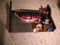
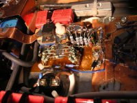
This picture shows the heart of the power stage. The power devices
are mount on a aluminium base plate. The base plate is isolated but
HF-connected to GND by 1nF (please refer to the schematic, where
“shielding” is mentioned.) Unfortunately the capton isolation looks quite similar
as copper and makes it harder to understand the construction from the pictures.
MosFet drains directly connected with 0.3mm copper foil
to the PFC diode. The cathode is again directly connected to foil
of the positive rail. The foil is splitted and carries the ferrite beads.
Below the foil of positive rail you can see the film cap.
Attachments
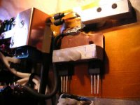
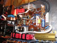
Next step is the GND foil. It is one origami foil that connects the film cap, the e-caps, the MosFet-source-resitors and the signal GND. Signal GND is the large copper area and no high currents are fed into this GND area. The signal GND foil carries the PFC chip, which is pressed with an additional GND strip onto the GND foil. ==> improved heat dissipation and optimized GND plane design in one step.
Attachments
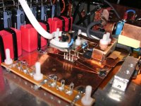
And now things are coming ugly for human perception ...all the small components in a three dimensional P2P set up....
You can see the source resistors (light green) providing the shortest connection to PWR_GND.
Behind the light blue resistors you might find the 5 PNP drivers for the MosFets.
And the snubber cap (consisting of four WIMA MKP10 2.2nF/2000V) coming from the drains and connected to the snubber diode which is directly soldered on the top of the PWR_GND.
Attachments
Here you can also see the discharge resistor of the snubber. The length of its connection is
uncritical (more or less...). In this set up the max. operation frequency at approx. 15W output power is around 100kHz and the snubber losses remain acceptable.
The three black sleeves carry several serial connected resistors, such as the 14x15k etc.
The sleeves are triple layered.
uncritical (more or less...). In this set up the max. operation frequency at approx. 15W output power is around 100kHz and the snubber losses remain acceptable.
The three black sleeves carry several serial connected resistors, such as the 14x15k etc.
The sleeves are triple layered.
Attachments
Eva said:Sorry, I had forgotten that you were using critical conduction mode. This is nice as to what concerns to switching losses since frequency goes down as current increases thus keeping losses under control.
Have you tried to place a 2.2nF (or maybe 1.5nF) capacitor directly between D and S pins of the switching device? The basic idea under that is to have an intentionally slow gate turn-on so that the capacitor charge peak current is kept low, and a relatively fast gate turn-off (but not fast enough to require a dozen of PNP buffers!). Such a capacitor in conjunction with MOSFET turn-off time and internal drain-source capacitance will limit rise time to approx 100ns even with 12A load, but in a less dissipative way, and shall ringing be present it would happen at fairly low frequencies (so little will be radiated). Note that your particular inductor design nicely allows for slow turn-on since the inductance is high for low currents, so inductor current rise in the first 500ns should be quite small, thus producing low losses.
The boost inductor will tend to resonate with that capacitor but I don't consider that as a problem.
Also, I would try these bead ferrites placed in the inductor side instead of the diode side. You shouldn't slow down diode commutation.
Hi Eva,
yes, I tried the cap directly between drain and source.
But this also slows down the downward sloping speed, which results in several drawbacks.
a) In general slow down sloping causes an increased time without reasonable current in the inductor, means I am leaving critical conduction mode and enter discontinous mode. Down sloping frequency is given by the inductor and the snubber cap and down sloping would become very slow....
b) but I tried it and found that the turn ON current peaks were harder than expected. The chip detects the turn ON timing, when the voltage across the choke is close to zero. The turn ON delay (some 300...600ns) should the hit the turn ON into a low drain source voltage voltage. Well with a large cap directly from drain to source - the turn ON hits into several hundreds volts drain source...
and discharges the caps with a heavy spike.
c) the chip seems to have issues with detecting very slow slopings and missed out several cycles especially at high input voltages (may be this could be fixed by more auxiliary turns on the choke).
d) this method was OK for snubber caps up to about 500pF, but 500pF still resulted in unacceptable fast du/dt at high loads.
Hm, seems like I have to live with the lossy snubber... or set up a completely new design...
But it looks to works acceptable now. As you already mentioned my stepped gap inductor prevents excessive operating frequencies and in combination with the additional power in the snubber (which also reduces fmax) .... it seems like I will typically not exceed 120kHz.
I would consider a dead time of 1us negligible at low operating frequencies like 25Khz to 35Khz. The corresponding periods are between 40us and 28us so 1us of dead time means almost nothing in efficiency terms (but it may solve all your EMI issues).
Also, 1us of deadtime combined with a slow rise time due to capacitor charging will help a lot to reduce maximum switching frequency with low loads. I would definitely take advantage of that fact if I was you, even at the expense of using a different control IC.
PD: The layout looks terrible
Also, 1us of deadtime combined with a slow rise time due to capacitor charging will help a lot to reduce maximum switching frequency with low loads. I would definitely take advantage of that fact if I was you, even at the expense of using a different control IC.
PD: The layout looks terrible
Terrible layout? Which layout?
Well, I don't care about "ugly inside".
But reliability might be a drawback, when considering that this PSU should operate inside a vibrating subwoofer...
I agree that 1us dead time would be fine.
But 2.2nF with 1.1mH will result in a natural resonance of 100kHz.
So theoretical sloping may take around 5us then, practically even more.
Already in the current design I am observing slow down sloping of around 3us....
But point b) & c) where my main reasons.
I also agree that for turn ON I could increase the impedance.
This would allow to bring down the turn ON current peaks, but
turn ON losses would be still defined by the hard switched energy.
For turn OFF, I expected to be able to work without PNP drivers,
but the low impedance was the only way which worked out without ringing in real life. Even with 2.2nF subber, this is the limit where I again observe starting issues during MosFet turn OFF.
With smaller snubber caps I simply did not manage to get a proper turn OFF, even not with that massive PNP driver.
My high heavy inductive load seems to interact with the MosFets
and gate drive in a very inconvinient way.
Hm,... should I really design a constant frequency PFC similar like yours?

Especially with your magnetic snubber this seems to be a nice solution that could handle wide range input, low load / full load,
and general high power much easier.
Or should I simply use my proto as long as it works?
...feeling some contradiction of my reliability demands vs
available DIY time...
Well, I don't care about "ugly inside".
But reliability might be a drawback, when considering that this PSU should operate inside a vibrating subwoofer...
I agree that 1us dead time would be fine.
But 2.2nF with 1.1mH will result in a natural resonance of 100kHz.
So theoretical sloping may take around 5us then, practically even more.
Already in the current design I am observing slow down sloping of around 3us....
But point b) & c) where my main reasons.
I also agree that for turn ON I could increase the impedance.
This would allow to bring down the turn ON current peaks, but
turn ON losses would be still defined by the hard switched energy.
For turn OFF, I expected to be able to work without PNP drivers,
but the low impedance was the only way which worked out without ringing in real life. Even with 2.2nF subber, this is the limit where I again observe starting issues during MosFet turn OFF.
With smaller snubber caps I simply did not manage to get a proper turn OFF, even not with that massive PNP driver.
My high heavy inductive load seems to interact with the MosFets
and gate drive in a very inconvinient way.
Hm,... should I really design a constant frequency PFC similar like yours?
Especially with your magnetic snubber this seems to be a nice solution that could handle wide range input, low load / full load,
and general high power much easier.
Or should I simply use my proto as long as it works?
...feeling some contradiction of my reliability demands vs
available DIY time...
Try an IGBT instead of a MOSFET, you may like the result.
Don't think that my magnetic snubber is going to solve all your problems, it may actually make things worse since it produces a nice 600V spike at turn-off (always within the avalanche ratings). It will probably cause a lot of trouble with MOSFETs, but IGBTs provide inherently limited rise times... and low capacitances... try them...
Don't think that my magnetic snubber is going to solve all your problems, it may actually make things worse since it produces a nice 600V spike at turn-off (always within the avalanche ratings). It will probably cause a lot of trouble with MOSFETs, but IGBTs provide inherently limited rise times... and low capacitances...
try them...Hi,
sorry, I also was under impression that your design is continious mode. The only experience I had with L6562 is very small flyback capacitor charger powered from 12V. Even so, the chip seemed a little touchy to me, especially when compared with very robust UC3843 from the same manufacturer. I rather use UC3843 as controller for discontinious flybacks. Frequency control requires addition of only one external npn from the reference to the CT pin, with R-C series connected from the base of the npn to the drain of the switching mosfet.
I also agree with Eva about IGBT. I once designed two transistor (asymmetrical half bridge) laboratory flyback capacitor charger working in discontinious mode. I used large IR mosfet modules, but they failed regularly, until I exchanged them for first generation of IGBTs in TO247 case. Peak current was 70A and charger is still working today.
Best regards,
Jaka Racman
Thanks to you both ! !
Great hint ! Sometimes I need some external help
to overcome my blindness....
I also think that an IGBT might be an interesting option.
Everybody is blaming them about their slow switching properties and especially their current tail.... But in my application this really could be
an advantage.
It might take again some time, but I plan to try it.
...hoping to come back with new results soon...
Markus
IGBT seem to be quite extraordinary for amateurs.
XXXXX has tons of them in their catalogue, but in the shop they had nothing, because "nobody is interested in buying that...".
Well, in finally he found one single IGBT. G4BC20U from International Rectifier, 600V/13A. Not powerfull enough for application, but worth a trial....
( Our professional electronic shops in Munich are closed on Saturday and currently I am not able to go shopping instead of work during the week......)
G4BC20U showed less ringing effects, but it was not possible to use a high driving impedance that would result in reasonable du/dt. During my ongoing tests I blowed the small IGBT and it took also the TDA4862 into death. Well, - I saw that an IGBT seems to match better to my requirements, but would not fully solve my issues.
I decided to improve the gate drive of my MosFets and go on with them. The new TDA4862 was more touchy than my first one (may be a fake?).
I tried one of the old L6560, which is now working alright after some adjustments.
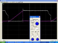
Improvement of gate drive: With the previous 27 Ohms between Chip and PNP driver was still some ringing at full power. It was clearly measurable that the output of the chip did not ring, while the base of the PNP already showed slight ringing and the MosFet gates again worse. Now with 10 Ohms this is fine and also the voltage and current wave forms of my MosFets are looking alright even at full power.
The white trace is the Drain voltage vs GND, 200V/Div.
The coloured trace is the current: 6,4A/Div.
Time base: 5us / Div.
XXXXX has tons of them in their catalogue, but in the shop they had nothing, because "nobody is interested in buying that...".
Well, in finally he found one single IGBT. G4BC20U from International Rectifier, 600V/13A. Not powerfull enough for application, but worth a trial....
( Our professional electronic shops in Munich are closed on Saturday and currently I am not able to go shopping instead of work during the week......)
G4BC20U showed less ringing effects, but it was not possible to use a high driving impedance that would result in reasonable du/dt. During my ongoing tests I blowed the small IGBT and it took also the TDA4862 into death. Well, - I saw that an IGBT seems to match better to my requirements, but would not fully solve my issues.
I decided to improve the gate drive of my MosFets and go on with them. The new TDA4862 was more touchy than my first one (may be a fake?).
I tried one of the old L6560, which is now working alright after some adjustments.
Improvement of gate drive: With the previous 27 Ohms between Chip and PNP driver was still some ringing at full power. It was clearly measurable that the output of the chip did not ring, while the base of the PNP already showed slight ringing and the MosFet gates again worse. Now with 10 Ohms this is fine and also the voltage and current wave forms of my MosFets are looking alright even at full power.
The white trace is the Drain voltage vs GND, 200V/Div.
The coloured trace is the current: 6,4A/Div.
Time base: 5us / Div.
Attachments
- Status
- This old topic is closed. If you want to reopen this topic, contact a moderator using the "Report Post" button.
- Home
- Amplifiers
- Power Supplies
- 1kW PFC-Boost