This is something that has been in the back of my mind for ages, but it was the thread a while ago about someone selling very expensive op-amps potted in copper tubes that prompted me to actually have a go at it...
The idea is to create a discrete op-amp small enough to directly replace a DIP8 IC op-amp, ideally surpassing the performance of one of similar cost (materials cost is ~£7 for a one-off, plus a few hours work). What has put me off trying before is the fact that to keep the footprint small enough it needs to be constructed entirely from SMT components, which are a pain to solder by hand.
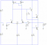
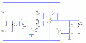
For the first attempt I wanted to keep it as minimalistic as possible to ensure that the size target was reachable. The resulting schematic is attached (shown in a non-inverting configuration). It is a standard 3-stage topology with absolutely no components not essential to operation. Ten components in total (Q1 and Q2 are a monolithic current mirror in a SOT143 package).
The input stage uses SST113 JFETs, which need to be matched (unfortunately I couldn't find any SMT dual JFETs) with a constant current diode in the tail and loaded with a current mirror. The current mirror has no degeneration resistors to reduce the component count by two. This means increased DC offset even with matched BJTs, so the LTP's degeneration resistors are replaced by a tiny potentiometer, allowing DC offset to be reduced to arbitrarily low levels.
The Vas uses a MOSFET (ZVP3306F) to present a high impedance to the input stage. It too is biased by a constant current diode. Dominant pole compensation encompasses the output stage rather than being taken from Vas output, which necessitates a larger value of capacitor and therefore lower slew rate and bandwidth but greatly reduced distortion, especially at higher frequencies.
The output stage is a complementary JFET source-follower, which is just about the simplest output stage possible.
The idea is to create a discrete op-amp small enough to directly replace a DIP8 IC op-amp, ideally surpassing the performance of one of similar cost (materials cost is ~£7 for a one-off, plus a few hours work). What has put me off trying before is the fact that to keep the footprint small enough it needs to be constructed entirely from SMT components, which are a pain to solder by hand.
For the first attempt I wanted to keep it as minimalistic as possible to ensure that the size target was reachable. The resulting schematic is attached (shown in a non-inverting configuration). It is a standard 3-stage topology with absolutely no components not essential to operation. Ten components in total (Q1 and Q2 are a monolithic current mirror in a SOT143 package).
The input stage uses SST113 JFETs, which need to be matched (unfortunately I couldn't find any SMT dual JFETs) with a constant current diode in the tail and loaded with a current mirror. The current mirror has no degeneration resistors to reduce the component count by two. This means increased DC offset even with matched BJTs, so the LTP's degeneration resistors are replaced by a tiny potentiometer, allowing DC offset to be reduced to arbitrarily low levels.
The Vas uses a MOSFET (ZVP3306F) to present a high impedance to the input stage. It too is biased by a constant current diode. Dominant pole compensation encompasses the output stage rather than being taken from Vas output, which necessitates a larger value of capacitor and therefore lower slew rate and bandwidth but greatly reduced distortion, especially at higher frequencies.
The output stage is a complementary JFET source-follower, which is just about the simplest output stage possible.
Attachments
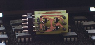
To best fit the circuit into the available space, I split it into two double-sided PCBs mounted parallel to each other. One contains the input stage, the other the Vas and output stage. The offset pot is sandwiched between the two boards, conveniently spacing them to exactly the width of a DIP8. Three jumpers physically bond the boards together.
A photo of the completed item is attached (stuck in a chip carrier to keep the pins straight). It's 12x20x9mm, excluding the pins. I could have squished it down to a smaller size, but I didn't want to push my luck on the first attempt; it's small enough anyway.
A photo of the completed item is attached (stuck in a chip carrier to keep the pins straight). It's 12x20x9mm, excluding the pins. I could have squished it down to a smaller size, but I didn't want to push my luck on the first attempt; it's small enough anyway.
Attachments
Performance is better than expected for such a simple circuit. Slew rate is a rather ordinary 10V/us, although I think I overdid the compensation capacitor, so higher should be reachable without problems (LTP current could also be increased from the present 1mA to the same end, but I want to keep quiescent current reasonably low). It's stable into capacitive loads of up to 1nF or so. I can't measure the bandwidth, but sims say the GBP should be around 36MHz with the 100pF compensation. Open-loop gain is about 120dB.
I can't yet make accurate THD measurements, but there is no discernible difference in distortion spectrum between the test signal from my soundcard (2nd harmonic at about -96dB, decreasing above that) and the op-amp output, so it can't be adding very much distortion. Sims say all harmonics are better than -160dB, or something ridiculous like that.
Noise is almost below my ability to measure too; it just pops up above the noise floor of my soundcard at -120dB (relative to 2V peak).
Output voltage swing is to within just a few tenths of a volt of the rails. Clipping is clean. Maximum supply voltage is about +/-18V.
Open-loop output impedance is about 40 Ohms. Input impedance is very high.
I'm pretty happy with how it's turned out.
Hi MrEvil,
the most read disadvantage of miller comp is the inability to source current from the LTP thus limiting slew rate.
A Less referenced disadvantage is the effect on sound quality.
Your 2 stage feedback is a similar toplogy that some writers have criticised.
Please comment on the pros & cons of 2 stage vs miller comp and on the sound quality of your discrete opamp.
What maximum output voltage at reasonable distortion can you achieve, +24dbu? (12.4Vrms).
>unfortunately I couldn't find any SMT dual JFETs
Linear Systems (www.linearsystems.com) has a variety of matched JFETs in SMD packages. And they would send you some samples. Unfortunately, none of them (or indeed any SMD JFETs I could find) comes close to 2SK389 / 2SJ109 in terms of low noise and high transconductance.
Patrick
Linear Systems (www.linearsystems.com) has a variety of matched JFETs in SMD packages. And they would send you some samples. Unfortunately, none of them (or indeed any SMD JFETs I could find) comes close to 2SK389 / 2SJ109 in terms of low noise and high transconductance.
Patrick
The disadvantage is reduced stability. The Vas needs to work hard at high frequencies to combat crossover distortion. I should have fitted a smaller compensation capacitor so I could experiment with different values of external compensation to see exactly how much is needed; with 100pF it's perfectly stable.AndrewT said:Please comment on the pros & cons of 2 stage vs miller comp and on the sound quality of your discrete opamp...
The advantage is reduced distortion. The gain of the Vas is used to reduce crossover distortion. Reduced crossover distortion can only be good!
Other than that it's virtually identical to normal Miller compensation.
As for how it sounds: It's the equal of any op-amp I've ever heard. Much better than cheap, common op-amps. I don't have any expensive op-amps spare to compare it with.
Distortion increases slowly as output increases towards clipping. At about 1V below the rails 2nd harmonic is about -70dB, higher harmonics decreasing smoothly. Above that level distortion rises fast. I'm not sure if that's what you would consider reasonable distortion.AndrewT said:...What maximum output voltage at reasonable distortion can you achieve, +24dbu? (12.4Vrms).
That's with +/-15V rails, giving 9.9Vrms. Assuming performance is similar with +/-18V rails (I don't want to push it to the limit since it's the only one I have right now) then that would be 12Vrms.
Note that it won't be able to drive heavy loads at that level or the output stage might be damaged.
They look interesting. I might see if they'll ship to the UK. They may not be as good as 2SK389 / 2SJ109, but then neither are the ones I'm using now.EUVL said:Linear Systems (www.linearsystems.com) has a variety of matched JFETs in SMD packages. And they would send you some samples. Unfortunately, none of them (or indeed any SMD JFETs I could find) comes close to 2SK389 / 2SJ109 in terms of low noise and high transconductance.
Patrick
Actually, going over the datasheets again I see it won't be able to get maximum output swing at +/-18V because although the n-JFETs (j113) are rated for 35V, the p-JFET (j177) is only 30V. So if it were used at +/-18V, an output swing greater than +12V peak might break something. Even if they were both rated 35V, swinging to within 1V of +/-18V rails would be right at the limit.
Other than that, the current diodes (SST505) are rated at 45V and the MOSFET (ZVP3306F) at 60V, which would limit the suppl voltage to +/-22V and +/-30V respectively.
The output current capability will vary depending on the exact specs of the output stage JFETs. In the worst case it will be about 9mA. Higher Idss/Vgs(off) devices may give 20mA. Minimum load impedance will be whatever doesn't exceed that.
Exceeding that current will cause the gate-source junctions to be forward biased and current will be drawn through the gate. In the negative direction this will be limited to 1mA by the current source, so no damage will occur (as long as the power rating is not exceeded). In the positive direction there is no limit. The maximum gate current is given as 50mA for j113, then it dies (much more than that and the MOSFET won't be too happy either).
Somewhat higher output current could be acheived by putting a resistor between the two gates of the output JFETs, with the n-channel one being attached to the negative side, the p-channel to the positive side. That would decrease quiescent current and increase the maximum output current before forward-biasing occured.
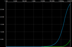
With all the talk about output impedance recently, I thought this might be interesting: It's a graph of simulated output impedance vs. frequency for normal Miller compensation (blue) and output-stage-inclusive compensation (green) at a non-inverting gain of ten.
Including the output stage in the compensation feedback loop gives an extra two decades of flat output impedance.
Including the output stage in the compensation feedback loop gives an extra two decades of flat output impedance.
Attachments
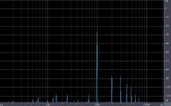
I can make better distortion measurements now, so here's an FFT of the output, 1kHz, 5V peak, 10K load, +/-15V supplies, non-inverting gain of 10. The fundamental is reduced by 30dB, so the actual relative amplitude of the harmonics can be read directly off the scale. THD is about 0.003%
It's not as good as I was hoping for; it only just manages to match an OPA604 and falls short of better op-amps. It does have much smoother clipping though.
I suspect that the output stage is responsible for much of the distortion. I'll try BJT and MOSFET output stages at some point.
It's not as good as I was hoping for; it only just manages to match an OPA604 and falls short of better op-amps. It does have much smoother clipping though.
I suspect that the output stage is responsible for much of the distortion. I'll try BJT and MOSFET output stages at some point.
Attachments
I've attached the schematic of the notch filter I used. Depending on how well tuned the twin-T filter is and the setting of the potentiometer, the notch can be very deep with very little effect on the amplitude of the harmonics. It does turn into a nice oscillator when too well tuned though, so a 30dB notch is about the best I have managed (which conveniently matches the 30dB overall gain), with perhaps 1dB attenuation of 2nd harmonic.
Attachments
Interesting
I am very interested to see where this goes as I have been considering a similair approach myself. If you can beat the ad8065/843/847 for sound quality that would be a stern test. Have you managed to get the slew up yet? I would need 14 units for my 2 headamps, preamp and phono stage")
Nick.
I am very interested to see where this goes as I have been considering a similair approach myself. If you can beat the ad8065/843/847 for sound quality that would be a stern test. Have you managed to get the slew up yet? I would need 14 units for my 2 headamps, preamp and phono stage
Nick.
Re: Interesting
I'm afraid you'll never be able to believe my opinions on the sound quality - I'm bound to say it's really goodbiovizier said:...If you can beat the ad8065/843/847 for sound quality that would be a stern test...
It would be hard to get the compensation capacitor out without breaking something, so I'll leave it for the next iteration, where I will increase the LTP current to 2mA and start out with a smaller capacitor of perhaps 10pF and increase it from there to achieve (unity gain) stability. I would like to reach 40V/us.biovizier said:...Have you managed to get the slew up yet?..
Don't expect me to go into production or anything... I think it would make me go crazy squinting at the tiny components all day! When I've finished I'll release PCB layouts and other details so anyone can make them.biovizier said:...I would need 14 units for my 2 headamps, preamp and phono stage
Nick.
40V/us is the sort of figure a good audio op-amp will give, so that's my target. It would be hard to go higher without losing stability or increasing distortion. I can't think of any situation where more would be needed anyway.
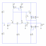
I've attached a schematic of what the next one will probably look like. MOSFET (NDC7002N) input stage since it's easy to get dual ones. There is a little space on the PCB, so added emitter resistors for the current mirror. Output stage changed to BJT, biased by diode-connected transistors. Using dual transistors for the output stage will result in automatic thermal compensation. It's been a struggle finding dual BJTs that are not in ludicrously small, unsolderable packages; I've finally settled on FMB100/FMB200 which should be possible to solder by hand.
I've attached a schematic of what the next one will probably look like. MOSFET (NDC7002N) input stage since it's easy to get dual ones. There is a little space on the PCB, so added emitter resistors for the current mirror. Output stage changed to BJT, biased by diode-connected transistors. Using dual transistors for the output stage will result in automatic thermal compensation. It's been a struggle finding dual BJTs that are not in ludicrously small, unsolderable packages; I've finally settled on FMB100/FMB200 which should be possible to solder by hand.
Attachments
In applications where the front-end of my discrete OPAMP’s circuits are exposed to large levels of RF – such as in DAC buffers / IV converters I’ve always found MOSFETS to be the best input devices.
Its well known that JFETs or degenerated Bipolar (not well known) should be used in positions where RF IMD products are expected at the input stage – however I’ve not seen anybody try MOSFET’s in these positions – maybe due to concerns over noise issues.
I use the Dual Vishay Si1900DL (also look at Si1901, 3, 6 etc) and operate these at 5mA a pair, at this level I’m able to achieve a SNR of better then 115dB Rel. 2Vrms – however watch there 30V voltage rating – a Cascoded input stage might be required (which also helps to reduce there input capacitance).
Later tests along the lines of Paul Millers RF IMD tests confirm the superiority of MOSFET’s as input devices – even surpassing the performance of JFETS – non degenerated Bipolar where appalling in this respect – interestingly, adding Emitter degeneration resistors to Bipolar front-end (always recommended anyway) dramatically improved there RF IMD performance – a fact I’ve never seen mentioned in print?
If you use MOSFET’s as input devices then I strongly recommend adding say 47R resistors directly on there Gates to insure “stability” – to "damp out" any tendency for the input stage to operate as a VHF Colpits oscillator.
A word of caution on SMD resistors – do not use 0603 resistors in audio applications – these are grossly non-linear with applied voltage – 0805 seem OK in this respect.
A small “hint” for mounting those ever shrinking SMT Devices, I’ve always been a “Hand Solder Pump person” but a seemly well kept secret (at least from me) is to use “Desoldering Braid” to remove solder bridges across fine pitch legs. I now “blob solder” all legs on say SC70 6pin devices, then use the Desoldering Braid to remove the excess – if you careful – you remove just enough to have perfect joints – works every time like a treat! (But hey, maybe everyone else already knows this?). It also works extremely well to remove old solder from the PCB during rework.
Also be aware that if you use Solder paste to mount SMT devices NEVER allow to get in contact with your skin – the lead particles within the past are so fine that they are readily absorbed by the skin directly into your blood stream. If like me, you’re not that careful when using nasty chemicals / products – do take care with this seemly "harmless" product.
When I look at your circuit – I wonder why you do not use a folded Cascode design – using the Dual packaged transistors BC846 / BC856 in SC70 would not increase the “package count” & the transistors are thermally matched where they need to be, but would significantly improved Slew rate performance – and being only “Dual stage” much easier to stabilize….
See attached PDF for a typical "simple" FC design - note the use of Dual packaged transistors to reduce the "component count".
Not the greatest design maybe, but trying to keep simple – the 100R resistors on the input pairs could be replaced by a pot to trim any DC offset. Hopefully by operating the output devices in Class A, they should not present the high-impedance Cascode stage with a non-linear load…. Output stage distortion can be reduced by C3 (& C2 depending on gain) a trick also used in the AD797.
John
Attachments
Thanks John. Lots if useful information there.
I did consider a folded cascode, as well as other topologies, but I decided to start out with the standard topology since it offers the most well-rounded set of compromises and it will serve as a benchmark for future experiments with other topologies.
I did consider a folded cascode, as well as other topologies, but I decided to start out with the standard topology since it offers the most well-rounded set of compromises and it will serve as a benchmark for future experiments with other topologies.
- Status
- This old topic is closed. If you want to reopen this topic, contact a moderator using the "Report Post" button.
- Home
- Amplifiers
- Solid State
- Miniscule discrete op-amp