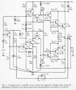
Today I launched my new website www.suplifier.nl. In this website I publish an article called “the Suplifier” which I wrote more than 15 years ago in a Dutch electronics magazine. Based on the principles of the Suplifier and on new insights, I moreover release now "The Ultimate Suplifier": a balanced input, DC coupled, symmetrical, bridge tied load, class A amplifier with no global feedback using transistors.
I open hereby the discussions on the theoretical starting points and the circuit of “The Ultimate Suplifier”, which you find on my website. I saw recently some threads and many posts on the issue of the output configuration. In “The Ultimate Suplifier” I propose, beside other new improvements, a brand new output configuration.
May I invite you all to give your comments on the principles and the circuit of “The Ultimate Suplifier”.
Marc.
http://www.suplifier.nl
Hi,
Good work! Looks like we are thinking similiarly.
The output stage I see on your website is
what I'd call darlington-sziklai, whereas the one I've
been interested in of late (shown in the thread 3 Different
Outputstage Driver Arrangements, Your Opinions!) is
what I'd call sziklai-darlington. Both are similiar but slightly
different depending on which part of the circuit has the sziklai.
The second (sziklai-darlington) is similiar to the Blomley amp.
I wonder if there are others out there who have investigated
these combinations. Seems to be more linear than triple
darlington. How do you like the sound?
Attachments
I like your output stage, it looks almost like a straight rip of the Threshold S300.
http://www.diyaudio.com/forums/attachment.php?postid=38107&stamp=1024679649
http://www.diyaudio.com/forums/attachment.php?postid=38107&stamp=1024679649
MFC,
I see a great difference between the output stage of the Blomley amp and what I propose. First the Blomley amp is no real Sziklai-darlington configuration. But moreover I think that an output stage must be only a current amplifier and for that reason it should be driven by the emitter of a transistor. As I see it well, the output stage of the Blomley amp, which starts with Tr7 and Tr8, is both a voltage and current amplifier.
I don’t understand your question about the limit to the number of devices you can place in a local feedback loop.
DJK an Georgehifi,
Yes, there is likeness to the output stage of the S300 MKII. I think that the emitter resistors R30-R41 will make the CFP work less well. Better is to place those resistor(s) in the collector as I did. But I understand why they did it this way. It is the only opportunity to place more than one output transistor parallel and to correct for the mutual differences between the output transistors. To my opinion it is not good to drive 6 !! output transistors by only one driver transistor. This must give much more distortion.
Marc.
http://www.suplifier.nl
Marc Vi. said:
Hi,
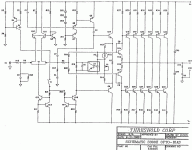
The Blomley has a sziklaii like the output stage (attached below)
not yours. Look at Tr8/10, Tr7/9 and mine Q2/Q3, Q6/Q5.
The similiarity between your output circuit and the attached is
that they have 3 transistors consisting of a sziklai and a
darlington in one case and a darlington and a sziklai in the other
case. The arrangement is different but a single stage is formed
from a compound of these two building blocks in both cases.
I see these "different" output stages being similiar. You can
call it different. I wasn't trying to start an argument about whose was better.
What I think these types of circuits do is provide more local
feedback then other configurations and can thus produce a more
linear stage. If you see something that I'm skipping over, please
elaborate more.
Especially useful for running in Class A with little to no global
AC feedback
")
Mike
Attachments
Mike,
I do agree that a three transistor output consisting of a Sziklai and a darlington is more linear and is especially useful for running in Class A with little to no global AC feedback. In this way your last attachment and my configuration are similar. And they are similar in the way that the output stage behaves like an emittor follower. But the Blomley amp output stage is not behaving like an emittor follower because the output stage is also voltage amplifying, if I see it correctly. And that makes a great difference. And, as I see it, the Blomley output stage is not a real Sziklai/darlington configuration but maybe that is of minor interest. But I am quite sure that without global NFB the Blomley amplifier and it’s output stage has a high distortion.
Marc.
http://www.suplifier.nl
The Blomley output stage is in no way behaving as an emitterfollower. The output is actually a current mirror with gain. Without overall feedback the ouput impedance would be quite high (as is the case with current mirrors).
It is maybe not directly clear to everyone, but the diodes D1 and D2 are the 'input transistors' of the current mirror. Tr7-11 and Tr8-12 are the 'output transistors' of the current mirror. The gain of the current mirror is 1000, which is the ratio R20/R17 or R21/R18. Tr 4 and 5 are the phase splitter of the amplifier.
The open loop voltage gain of this amplifier depends a lot on the load it sees and changes with changing load impedance (like a loudspeaker).
The ouput of Marc's suplifier is behaving as an emitterfollower, and a quite linear one.
Steven
Steven said:The Blomley output stage is in no way behaving as an emitterfollower...
Hi Steven,
Hmmm...looks like I need to study the Blomley more. Take a look
at Marks output -vs- the output stage I posted in #8. You see the
similiarity there? Both are acting as emitter followers (very linear).
Now take a look at my output stage and the Blomley. Mine is
a sziklai-darlington, and when I look at the Blomley, I see the
same thing (although it uses PNPs where I use NPNs and NPNs
where I use PNPs).
So follow this train of thought for a moment...I could take a diode
and add it to the input of my output stage (similiar to Blomley),
and it would not be acting as an emitter follower either? If this is
the case, then can't the Blomley be seen as a sziklai-darlington
configuration that isn't acting like an emitter follower?
I'm trying to learn something here because the Blomley looks
very similiar to my output stage.
Mike
Hai Marc,
Went through your site and enjoyed reading it very much. The Ultimate Suplifier is a pretty good looking design. But how does it sound? Can you report any comparisons?
Some of the sub-pages seem to have errors as they fail to open.
Finally, what is the output power and do you have any PCB design to try it out?
Thanks,
mfc said:
Hmmm...looks like I need to study the Blomley more. Take a look
at Marks output -vs- the output stage I posted in #8. You see the
similiarity there? Both are acting as emitter followers (very linear).
Now take a look at my output stage and the Blomley. Mine is
a sziklai-darlington, and when I look at the Blomley, I see the
same thing (although it uses PNPs where I use NPNs and NPNs
where I use PNPs).
So follow this train of thought for a moment...I could take a diode
and add it to the input of my output stage (similiar to Blomley),
and it would not be acting as an emitter follower either? If this is
the case, then can't the Blomley be seen as a sziklai-darlington
configuration that isn't acting like an emitter follower?
Hi Mike,
The Blomley is not working as you think it does. But first to your output in #8 and Marc's one.
Your output is a Sziklai pair with a darlington as the second transistor. It behaves as a quite linear single transistor. You have one Vbe drop from input to output, the one from Q3 (or Q6). It has one loop from input to output, i.e. the collector of the output transistor(s) is connected to the emitter of the input transistor.
Marc's output is a single emitter follower, followed by a Sziklai pair. It behaves as a quite linear darlington. It has two Vbe drops from input to output, Q13+Q15 or Q14+Q16. In this case the feedback loop is around two transistors and chances are that this circuit is more stable than yours.
Back to the Blomley.
In the Blomley circuit the diodes D4 and D5 are not biasing the output stage, but is biasing the phase splitter Tr4+Tr5. C3 keeps D4 and D5 at a stable DC point, so it will not move. The current output of the amplifier Tr3 and Tr6 is bidirectional, i.e. it can source (through Tr6) and sink current (through Tr3). Tr6 is actually just a DC current source and Tr3 is doing the current modulation. As Tr5 can only sink current and Tr4 can only source current, here phase splitting takes place. Here is the class B switching done at an early stage by fast small signal switching transistors, Tr5 and 4. Through Tr5 half of the current flows, let's call it the positive half. Through Tr4 the other half of the current is flowing, the negative half. There is hardly any voltage swing, only current.
The positive half needs current amplification by a 1000:1 current mirror. The mirror consists of D1 as input transistor with R20 as 'sort of' mirror emitter resistor and Tr7,9,11 as output transistor with R17 as mirror emitter resistor. The current ratio is R20/R17 (1000). The voltage drop of D1 is cancelled by Vbe of Tr7. Tr9 and Tr11 are enhancing the current capabilities of Tr7 and, yes, Tr7..11 is a Sziklai with darlington as second transistor, just like your circuit. The difference is that in your circuit that compound transistor is used as emitter follower, but in the Blomley that compound transistor is used upside down as 'collector follower', part of the current mirror. The emitter of Tr11 behaves as the collector (!) of the PNP compound transistor, while the emitter of the compound transistor is the collector of Tr11, that is connected to R17.
Because the load is connected to the collectors of the compound transistors (the current outputs of the mirrors), the output impedance is determined by the load resistor itself. Without load the impedance is quite high. Only feedback will lower the output impedance.
In your #8 circuit the output impedance will be quite low due to the emitter follower action, even in open loop, if the output stage is driven from a source with a not too high impedance., e.g. a resistor loaded VAS.
BTW, R11 in the Blomley circuit sets a DC bias current in the ouput stage, so that even with no input signal a DC current is flowing in the output. The output itself never switches off! No switching distortion here. As said the switching is done in the previous stage already. Here switching distortion may occur, but these transistors can switch a lot faster. That is the strong point of the Blomley stage.
Steven
Hi Marc Vi.
You are very thorough (I dare to say pedantic) about keeping all stages as linear as possible without global feedback. I guess your suplifier is one of the 'lowest THD' no global feedback amplifiers. It is impresing to see how much work on details you have spent.
Tell me what is the purpose of C4a/b and C5a/b ??
Are you affraid of Q9 and Q10 stability on capacitive load? No idea- it looks like a compensation of non-existing feedback to me
regards
Hi Darkfenriz,
Thank you, my goal was and is indeed to make each stage as linear as possible.
The purpose of C4a/4b and C5a/5b is to filter out HF signals picked up out off the air or HF ringing signals and to avoid this signals being amplified and reaching the output stage.
Marc.
Thank you, my goal was and is indeed to make each stage as linear as possible.
The purpose of C4a/4b and C5a/5b is to filter out HF signals picked up out off the air or HF ringing signals and to avoid this signals being amplified and reaching the output stage.
Marc.
Hi Steven,
Thanks for the analysis (analysees?). The Blomley inner workings
and how it first appears to work with a quick glance at the
schematic are very different. I haven't digested your analysis
on the Blomley yet. Will do so this weekend.
I was playing around with some simulations of the darlington
sziklai (Marc's) and the sziklai darlington (mine). .
Yes, i've seen that the darlington sziklai is more stable.
However, its not too bad to stabilize the sziklai darlington.
Yes, the sziklai darlington has very low output impedance and
works well into 4 ohms. From what I tried, the darlington sziklai
(Marc's) has to have the resistor (.22 ohm) in series which raises
the output impedance compared to the sziklai darlington. I
lowered the .22 ohm resistor to .1 ohm and then .03 ohms and it
started behaving better into 4 ohms. It looses some gain
depending on the size of this resistor.
Both circuits have excellent distortion profiles in my amp circuit.
They show a distortion pattern that monotonically decreases with
order when run full out (in this particular circuit). The sziklai
darlington is a bit more linear in that the distortion pattern is a
little lower in magnitude. I like a distortion profile that
monotonically decreases with order (my particular bias).
Both circuits are better in my amp than than the triple darlington
which I can't get to have this monotonically decreasing profile at
max signal input.
Thanks,
Mike
Thanks for the analysis (analysees?). The Blomley inner workings
and how it first appears to work with a quick glance at the
schematic are very different. I haven't digested your analysis
on the Blomley yet. Will do so this weekend.
I was playing around with some simulations of the darlington
sziklai (Marc's) and the sziklai darlington (mine). .
Steven said:
<Much good stuff on the Blomley snipped...>
...chances are that this circuit is more stable than yours.
Yes, i've seen that the darlington sziklai is more stable.
However, its not too bad to stabilize the sziklai darlington.
In your #8 circuit the output impedance will be quite low due to
the emitter follower action, even in open loop, if the output stage
is driven from a source with a not too high impedance., e.g. a resistor loaded VAS.
Yes, the sziklai darlington has very low output impedance and
works well into 4 ohms. From what I tried, the darlington sziklai
(Marc's) has to have the resistor (.22 ohm) in series which raises
the output impedance compared to the sziklai darlington. I
lowered the .22 ohm resistor to .1 ohm and then .03 ohms and it
started behaving better into 4 ohms. It looses some gain
depending on the size of this resistor.
Both circuits have excellent distortion profiles in my amp circuit.
They show a distortion pattern that monotonically decreases with
order when run full out (in this particular circuit). The sziklai
darlington is a bit more linear in that the distortion pattern is a
little lower in magnitude. I like a distortion profile that
monotonically decreases with order (my particular bias).
Both circuits are better in my amp than than the triple darlington
which I can't get to have this monotonically decreasing profile at
max signal input.
Thanks,
Mike
mfc said:
Yes, the sziklai darlington has very low output impedance and
works well into 4 ohms. From what I tried, the darlington sziklai
(Marc's) has to have the resistor (.22 ohm) in series which raises
the output impedance compared to the sziklai darlington. I
lowered the .22 ohm resistor to .1 ohm and then .03 ohms and it
started behaving better into 4 ohms. It looses some gain
depending on the size of this resistor.
Mike,
You shoudn't compare your own 'sziklai darlington' without emitter resistors and Marc's 'darlington sziklai' (your nomenclature) with emitter resistors. Both circuits need emitter resistors to keep the bias current stable over temperature. Your 1.2 Ohm emitter resistors are only used for equal current sharing and do not help much in keeping the bias current stable. For that purpose you need an 'emitter resistor' from the common collector junction of the output transistors and the driver and the emitter of the pre-driver. This compound transistor behaves like a single transistor with the polarity of the pre-driver (NPN or PNP), so this compound transistor needs an emitter resistor to the load. Try some different bias voltages in your simulation and you will see what I mean.
Steven
Steven said:
...
Both circuits need emitter resistors to keep the bias current stable over temperature...
Hi Steven,
Thanks for your analysis on this. Didn't realize
I had stacked the deck against the darlington sziklai.
Regarding thermal issues of these compound stages...I'm not
aware of any literature on them, so I'd like to see what you
think about getting the sziklai darlington thermally stable.
How big or what percentage of the one diode drop from the preDriver
transistor should the emitter resistor be?
Can I avoid the emitter resistor and still be ok thermally?
Reason to avoid emitter resistor is that it really messes up the
distortion profile. How about:
a) running as low a current thru the first transistor (preDriver)
as possible to avoid large thermal fluctuations in its Vbe.
b) relying on a Vbe multiplier
Thanks,
Mike
Hi Mike,
Getting a Sziklai darlington thermally stable is not a bigger problem than a normal darlington; on the contrary, it should be quite easy. The temperature of the predriver and the temperature matching with the Vbe multiplier, combined with the voltage drop across the emitter resistor to the load determines the stability. The bigger the voltage drop across the emitter resistor, the more stable. Since the predriver will have less variations in temperature than the output transistors, it can be expected that this configuration is more stable than a normal darlington, where also the Vbe variations over temperature of the output transistors should be cancelled by the Vbe multiplier.
I think a minimum of around 25mV across the emitter resistor is required for temperature stability, so the Re value depends on the bias current you want to set. More is better for stability. Take into account that the Vbe of a bipolar Si transistor changes 2mV per degree C or K. Vbe decreases (with constant Ic) for increasing temperature. So a small temperature diifference between the Vbe multiplier transistor and the predriver already makes a big difference in bias current.
There are ways to avoid the emitter resistor but these require more components. You could do current sensing via a resistor on the other side of the output transistor (e.g. your 1.2 Ohm resistors) and adjust the bias voltage accordingly, but this is not so easy since the voltage across that resistor is also influenced a lot by the actual audio signal. So some processing needs to be done to remove that part.
Steven
- Status
- This old topic is closed. If you want to reopen this topic, contact a moderator using the "Report Post" button.
- Home
- Amplifiers
- Solid State
- The Ultimate Suplifier