Steven said:
...I think a minimum of around 25mV across the emitter resistor is required for temperature stability
Hi Steven,
I ran some simulations of the distortion for various values of
emitter resistor. In class A, the idle is about 5.5 amps/60v.
A 4 ohm load is worst case behavior, and in this situation,
in order to keep a good profile of distortion, the max value of
the emitter resistor needed to be less than .01 ohms. So
5.5amps x .01 = 55mv.
Curious how you came up with 25mv? Note just for comparison,
a 10amp AGC-10 fuse at rated current has approximately a
200mv drop across it at 25 degrees C.
I increased the preDriver resistors from 300 ohms to 10k. This
lowered the current in the predriver from 8ma down to 1ma
without any problem. So the predriver will dissipate about
60mwatts (the KSC1845 is rated at 500mwatts).
I think this sounds like it will work, but was wondering what
you thought.
Thanks,
Mike
Mike,
The 25mV is based on the optimum bias current for class AB emitter follower output stages. Although this is optimum w.r.t. minimum deviations in output resistance from no load to max load, many people prefer to have more bias current (idle current). This value of 25mV is rather low with respect to temperature stability, but workable if the Vbe multiplier is kept at the same temperature as the transistors that determine the bias current of the output. These can be the output transistors themselves (e.g. darlington) or the driver (sziklai) or the predriver (sziklai darlington). If heatsinking is mediocre, then better take more than 25mV.
BTW 5.5A is a BIG bias current and avoid fuses in the output.
Steven
Steven,
You wrote:
Does this mean that for class A, where the bias current is let say 1,2 A, the value of the emitter resister Re can be lowered down to 25mV/1,2A = 0,022 ohm instead of normally 0,22 ohm? This may be important for an amplifier without (global) NFB or error correction because in that case the damping factor is limited by the value of Re.
Marc.
You wrote:
a minimum of around 25mV across the emitter resistor is required for temperature stability, so the Re value depends on the bias current you want to set. More is better for stability.
Does this mean that for class A, where the bias current is let say 1,2 A, the value of the emitter resister Re can be lowered down to 25mV/1,2A = 0,022 ohm instead of normally 0,22 ohm? This may be important for an amplifier without (global) NFB or error correction because in that case the damping factor is limited by the value of Re.
Marc.
Steven
what you say about voltage drop on emitter resistors is pretty reasonable, but this assumes, that output transistors are driven by good (low Z) voltage source, which is frequently far from truth (especially in projects with ccs-loaded vas....drivers....O/P).
My point is: do we really have to worry about output R when it is fairly low and use relatively higher emitter resistors for emitter feedback (degeneration)?
Marc Vi. said:
Does this mean that for class A, where the bias current is let say 1,2 A, the value of the emitter resister Re can be lowered down to 25mV/1,2A = 0,022 ohm instead of normally 0,22 ohm? This may be important for an amplifier without (global) NFB or error correction because in that case the damping factor is limited by the value of Re.
If the voltage drop across the emitter resistor is in the range of (only) 25mV, depending on the dimensioning of the heatsink and the thermal coupling between Vbe multiplier and the output transistors (or drivers for Sziklai), the idle current may vary as much as 50% or even more. For a class AB amplifier this is not such a big problem, except that the current may not be optimum anymore and some additional distortion might be generated, but for a class A amplifier with an idle current of 1.2A such a 50% change in bias current cannot be tolerated that easily. It could mean that the amplifier becomes underbiased and cannot deliver the required current (depending on toplogy) or that the amplifier becomes overheated. For a class A amplifier there is almost no such thing as optimum bias current, such as is the case for class AB. Both halves of the class A output stage are conducting all the time, keeping the transconductance quite stable, whereas in class AB the transconductance will vary with the signal, and an optimum bias current can be found. For that reason the value of the emitter resistor and the value of the bias current are more or less independent for class A and more than 25mV is no problem for distortion. For temperature stability more than 25mV will be wise. A value of 200mV should be enough, anyway. And this can be set easily with the normal values of 0.1 to 0.22 Ohm. In open loop amplifiers this will still result in a reasonable to good damping factor. Top and bottom half are in parallel (for class A), so with 0.22 Ohm, the DF is still 8/(0.22//0.22), so approximately 80 for an 8 Ohm load.
Steven
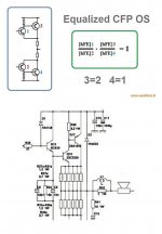
equalized CFP Output Stage
ciao
inside CFP there is a big gain
that is an "HIDE GAIN" because at last global gain is 1
but if you see the single gain of each device
this are different and different is the speed in each rail
my idea is using the same devices of final as driver
that build an equalized CFP Output Stage

in picture there is an axample of Suplifier Modification
ciao
inside CFP there is a big gain
that is an "HIDE GAIN" because at last global gain is 1
but if you see the single gain of each device
this are different and different is the speed in each rail
my idea is using the same devices of final as driver
that build an equalized CFP Output Stage
in picture there is an axample of Suplifier Modification
Attachments
Today I launched my new website www.suplifier.nl. In this website I publish an article called “the Suplifier” which I wrote more than 15 years ago in a Dutch electronics magazine. Based on the principles of the Suplifier and on new insights, I moreover release now "The Ultimate Suplifier": a balanced input, DC coupled, symmetrical, bridge tied load, class A amplifier with no global feedback using transistors.
I open hereby the discussions on the theoretical starting points and the circuit of “The Ultimate Suplifier”, which you find on my website. I saw recently some threads and many posts on the issue of the output configuration. In “The Ultimate Suplifier” I propose, beside other new improvements, a brand new output configuration.
May I invite you all to give your comments on the principles and the circuit of “The Ultimate Suplifier”. Marc. http://www.suplifier.nl
This weblink don't goes open. also about webarchive I don't get informations.
Last edited:
Sorry, tiefbassuebertr, but the website doesn't exist any longer. I'll mail you the content. Marc Vi.
Many thanks for sending me this thick bound of circuit informations - If I have study the schematics, I let you know more about my estimations.
It is curious for me, that the schematics and text files could not be found about
Internet Archive: Wayback Machine
only this message was shown:
http://web.archive.org/web/*/http://www.suplifier.nl
Last edited:
The Blomley output stage is in no way behaving as an emitterfollower. The output is actually a current mirror with gain. Without overall feedback the ouput impedance would be quite high (as is the case with current mirrors).
It is maybe not directly clear to everyone, but the diodes D1 and D2 are the 'input transistors' of the current mirror. Tr7-11 and Tr8-12 are the 'output transistors' of the current mirror. The gain of the current mirror is 1000, which is the ratio R20/R17 or R21/R18. Tr 4 and 5 are the phase splitter of the amplifier.
The open loop voltage gain of this amplifier depends a lot on the load it sees and changes with changing load impedance (like a loudspeaker).
The ouput of Marc's suplifier is behaving as an emitterfollower, and a quite linear one.
Steven
Dear Steven and dear all,
To make the discussion a bit more easy I did a redraw of the original Blomley design (WW 1971).
Hans
Attachments
- Status
- This old topic is closed. If you want to reopen this topic, contact a moderator using the "Report Post" button.
- Home
- Amplifiers
- Solid State
- The Ultimate Suplifier