I've been reading Randy Slone's "High-Power Audio Amplifier Construction Manual", which I picked up right after reading Douglas Self's amplifier design book. Douglas Self described some distortion reduction techniques for the VAS, including having a beta-enhancing emitter follower at the VAS input, as well as using a cascode at the VAS output. These designs were used in conjunction with an input stage diff amp having a current mirror load to balance it. I was disappointed that Self didn't provide data on the combination of the beta enhancement and cascode techniques (it was an "either or" option), nor did he discuss any complementary versions of his circuit at all. In fact, he acts as if fully complementary designs don't even exist. I don't think he ever mentions them at all.
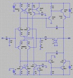
On reading Slone's book, I was quite happy to find that not only did he have a fully complementary design using current mirrors on the diff amp outputs, but also combined this approach with both a beta-enhanced VAS input and a cascoded VAS output. Nice! That is, it was nice until I tried to calculate the bias current of the last transistor of the VAS. Then I realized there was a serious flaw in the design. That bias current is subject to large variations and is essentially uncontrolled. To illustrate, I've modified his design a little bit with different current sources and resistor values to avoid copyright issues, but preserved the basic topology. I entered the schematic into LTSpice, and I show the schematic below. It's easy to see how to calculate the currents in the diff amp of course. Likewise, the emitter follower bias current can be easily seen to be one Vbe drop divided by its emitter resistor. No problem. But check out that last stage! How do you calculate its bias current? LTSpice calculates a value of about 50 mA, which is close to the value Slone reports, but it's not clear how this happens. Apparently it just rises until it loads down the emitter follower enough that it can't support any further rise. As an experiment, I tried raising the supplies to +/-90 V from +/-60 V. The VAS output stage bias current goes from 50 mA to 140 mA. That's really bad.
I began to think that the whole idea of using current mirrors on the diff amp outputs of a fully complementary design was a terrible idea. You end up with the diff amp output being taken from back-to-back collectors, so the voltage at that point is no longer controlled. Self avoids this problem with a single-ended design by biasing the VAS with a constant-current load. So the voltage at the diff amp output is controlled by the Vbe drops of the VAS, plus the forced VAS current times the VAS emitter resistor, and the current of the VAS is forced by a constant-current load. But with a fully complementary design, this isn't possible.
Is it possible somehow to use current mirror diff amp loading with a fully complementary design and still get stable, easily controllable VAS bias current? It turns out that you can. I'll show a schematic in the next post.
Attachments
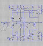
The key to fixing this problem is with the emitter followers in the current mirror. Now, instead of using the smallest resistors possible in the current mirror, I make them larger to provide a voltage large enough to bias subsequent stages with stable performance. So the diff amp currents set the voltage across the current mirror resistors to about 1.3 Volts. Then there's two Vbe drops down to the current mirror output voltage, which is now set to a stable value. Subsequent stages can now be biased just as if the design had collector resistors instead of a current mirror.
I'm sure I'm about the bazillionth person to rediscover this technique. But since a circuit with a significant design flaw appeared in a book that some may use to build their amps, I thought I'd bring it up and maybe save someone some trouble.
I'm sure I'm about the bazillionth person to rediscover this technique. But since a circuit with a significant design flaw appeared in a book that some may use to build their amps, I thought I'd bring it up and maybe save someone some trouble.
Attachments
andy_c said:The key to fixing this problem is with the emitter followers in the current mirror. Now, instead of using the smallest resistors possible in the current mirror, I make them larger to provide a voltage large enough to bias subsequent stages with stable performance. So the diff amp currents set the voltage across the current mirror resistors to about 1.3 Volts. Then there's two Vbe drops down to the current mirror output voltage, which is now set to a stable value. Subsequent stages can now be biased just as if the design had collector resistors instead of a current mirror.
I'm sure I'm about the bazillionth person to rediscover this technique. But since a circuit with a significant design flaw appeared in a book that some may use to build their amps, I thought I'd bring it up and maybe save someone some trouble.
Refreshingly original...
") .......you may want to run an AC analysis to rapidly determine whether or not the two designs have identical ft's, everything else being constant....
.......you may want to run an AC analysis to rapidly determine whether or not the two designs have identical ft's, everything else being constant....this should at least give you a clue as to whether your modifications actually function as true current mirrors....
Further confirmation can be gleaned by also running a slew rate test....using an ideal differentiator, (if your LT spice has one?) at the transimpedance stage's output......
If the results from this are in close agreement with the theoretical slew, then you may very well be onto a winner....good luck!
Well, it didn't work out. AC analysis showed the circuit in the Slone book to have a gain-bandwidth product matching the theory almost exactly. My circuit was low by a factor of almost 4, and it wasn't an integer ratio either. Very strange. When I tried to do a transient analysis with the Slone circuit, LTSpice went nuts, showing a local parasitic oscillation somewhere that I could not kill (I didn't try that hard though). Then I went back to resistive bias in my circuit and all was well with both the theoretical gain-bandwidth product vs the simulated, and the convergence of the transient analysis. But the benefits of diff amp balancing from the current mirror are lost with the resistive bias. That stinks. There has to be a way to get the current mirror to work in a fully complementary design while allowing a stable, predictable, controllable bias current in the VAS.
I'm amazed that the author allowed a design with an uncontrolled VAS bias current to not only be published at all, but to describe it as some kind of state-of-the-art design. Just because it has ultra-low measured distortion doesn't necessarily mean all is well.
I'm amazed that the author allowed a design with an uncontrolled VAS bias current to not only be published at all, but to describe it as some kind of state-of-the-art design. Just because it has ultra-low measured distortion doesn't necessarily mean all is well.
With all due deference to my college......
It is refreshingly original all right, but unfortunately does not appear to be a current mirror any more with the addition of the two additional transistors. As such the voltage gain is not high as in a conventional current mirror. In fact I don't believe it work in the circuit, and most likely has too little voltage gain as a load for the diff pairs. An active collector load is going to have a high voltage gain and likely more sensitivity to shift in quiescent current from supply changes than a resistor collector load. Increasing the emitter resistors for the current mirror in the first schematic to get the same voltage at the collector of Q1 and Q3 and adding the degeneration resistors to Q14 and Q18 will give a higher gain for the first stage and a lower gain for the second stage due to the degeneration resistors. I can't definitely say but would think that it would lessen the current sensitivity to supply voltage.
The poles (Ft is usually used to denote the point where the Hfe drops in a transistor and is a factor the frequency of the poles but is not the only influence) should move from these changes as well since the gain of both stages will be changed by the larger (and added) emitter resistors. You will have less current change from temperature with the additional degeneration and greater linearity in the open loop gain. I can't read the component values well enough to duplicate your simulation. Resistor loads for the first stage would lower this sensitivity but also lower the open loop gain which might not be a bad idea. This circuit has very large amount of open loop gain as it stands now. Resistors can be used in conjunction with the current mirrors to allow changes in gain, without large changes in the gain transistors quiescent currents. Not everyone agrees this much loop feedback is necessary or sounds better. Further degeneration for the diff amp current sources would probably help reduce the quiescent current changes. This really may not be an issue as your supply voltages should not change anywhere near as much as the range you mentioned.
You need floating current sources in the VAS collectors, to define their bias current/s to make use of current mirror diffa amp loads in fully complementary designs. I do think there is a horribly complex design that does have these added. I just have to try and remember where I had seen it.
Lukas
Lukas
Fred,
Yes, you are right-it's not a true current mirror anymore. For some odd reason, the gain-bandwidth product is 3.2 times less with the emitter followers present. I would have expected that ratio to be either 2 or 4. Just chalk it up as one of those nice ideas that didn't pan out, I guess.
I saw mikek's odd use of "ft" and just assumed he meant "gain bandwidth product" (gm/C). Testing that actually turned out to be a simple way to verify that the circuit really wasn't doing what I thought it was doing.
I'm aware that the DC open-loop gain of the circuit is high, and familiar with the history of those issues.
In fact, there's a (rather boring) story behind this. Back when I was a big party guy in the mid '70s, I decided to become an EE after reading Dr. Leach's article in Audio on TIM distortion. That was a great mag back then. I ended up going to school there, and was a student of his in the late '70s. After looking at those issues myself, I realized that some of the conclusions of Ottala's and Leach's articles were incorrect. Take the treatment of the transfer function from amp input to differential input for example. A lot of emphasis was placed on the ratio of the max to min value of that transfer function. That ratio is (1 + A0 * B) where A0 is the DC open-loop gain and B is the feedback factor. Even though you can reduce that ratio by reducing the DC open-loop gain, the maximum value (at "infinite" frequency) is still 1. And that's what overloads the input stage. The key seems to be creating an input stage that's robust in the presence of high peak error-correction signals.
Later on, I concluded that current feedback was the answer. After all, the input stage of a current feedback amp is linear with regard to current output up to the point of self-destruction or externally imposed current limit. It can handle error correction signals as large as you'll ever see. So I worked on a current feedback design and was almost ready to build it. Then I found out how to do distortion analysis with LTSpice using .FOUR. The full-power high-frequency distortion of the "VAS" (and I use that term for lack of a better one, as an analogy only) of the current feedback design sucked. After reading some of the standard texts on amplifier design (Self, I almost hate to admit), I realized what was going on. In the standard voltage feedback design, the local feedback in the VAS via the integration capacitor increases with frequency, essentially canceling out the distortion increase caused by the reduction of overall NFB with increasing frequency that occurs at the same rate. But the current feedback arrangement has a capacitor from output to ground in its "VAS". So its distortion at high frequencies goes up because of the load, while the amount of negative feedback at high frequencies goes down. This causes a "double whammy" with high-frequency distortion in the current feedback design. I was essentially failing to see some of the elegant, yet subtle features of the classic voltage feedback power amp design. So I scrapped the current feedback design. I really would't have cared if the simulated distortion had been a few tenths of a percent. But it was getting to the one percent region. That sucks.
So my goal now is to go through a distortion optimization process using designs somewhat like the hardcore objectivists are advocating. Then, I'll reduce the NFB such that I can get a large-signal square wave response with no overshoot with highly capacitive loads and no output inductor. The idea is that the reduction in NFB will not cause the amp to have obscene levels of distortion, because I started with a configuration that had extremely low distortion to begin with. That's where I'm headed at the moment.
Yes, you are right-it's not a true current mirror anymore. For some odd reason, the gain-bandwidth product is 3.2 times less with the emitter followers present. I would have expected that ratio to be either 2 or 4. Just chalk it up as one of those nice ideas that didn't pan out, I guess.
I saw mikek's odd use of "ft" and just assumed he meant "gain bandwidth product" (gm/C). Testing that actually turned out to be a simple way to verify that the circuit really wasn't doing what I thought it was doing.
I'm aware that the DC open-loop gain of the circuit is high, and familiar with the history of those issues.
In fact, there's a (rather boring) story behind this
. Back when I was a big party guy in the mid '70s, I decided to become an EE after reading Dr. Leach's article in Audio on TIM distortion. That was a great mag back then. I ended up going to school there, and was a student of his in the late '70s. After looking at those issues myself, I realized that some of the conclusions of Ottala's and Leach's articles were incorrect. Take the treatment of the transfer function from amp input to differential input for example. A lot of emphasis was placed on the ratio of the max to min value of that transfer function. That ratio is (1 + A0 * B) where A0 is the DC open-loop gain and B is the feedback factor. Even though you can reduce that ratio by reducing the DC open-loop gain, the maximum value (at "infinite" frequency) is still 1. And that's what overloads the input stage. The key seems to be creating an input stage that's robust in the presence of high peak error-correction signals.Later on, I concluded that current feedback was the answer. After all, the input stage of a current feedback amp is linear with regard to current output up to the point of self-destruction or externally imposed current limit. It can handle error correction signals as large as you'll ever see. So I worked on a current feedback design and was almost ready to build it. Then I found out how to do distortion analysis with LTSpice using .FOUR. The full-power high-frequency distortion of the "VAS" (and I use that term for lack of a better one, as an analogy only) of the current feedback design sucked. After reading some of the standard texts on amplifier design (Self, I almost hate to admit), I realized what was going on. In the standard voltage feedback design, the local feedback in the VAS via the integration capacitor increases with frequency, essentially canceling out the distortion increase caused by the reduction of overall NFB with increasing frequency that occurs at the same rate. But the current feedback arrangement has a capacitor from output to ground in its "VAS". So its distortion at high frequencies goes up because of the load, while the amount of negative feedback at high frequencies goes down. This causes a "double whammy" with high-frequency distortion in the current feedback design. I was essentially failing to see some of the elegant, yet subtle features of the classic voltage feedback power amp design. So I scrapped the current feedback design. I really would't have cared if the simulated distortion had been a few tenths of a percent. But it was getting to the one percent region. That sucks.
So my goal now is to go through a distortion optimization process using designs somewhat like the hardcore objectivists are advocating. Then, I'll reduce the NFB such that I can get a large-signal square wave response with no overshoot with highly capacitive loads and no output inductor. The idea is that the reduction in NFB will not cause the amp to have obscene levels of distortion, because I started with a configuration that had extremely low distortion to begin with. That's where I'm headed at the moment.
andy_c said:There has to be a way to get the current mirror to work in a fully complementary design while allowing a stable, predictable, controllable bias current in the VAS.
There is actually.....read about it soon in electronics world....
What is the point in tying to cascode the VAS stage anyway?
The capacitor going from the output back to the input sets the dominant pole. The cascode stage now has the same bandwidth as the common emitter stage. A cascode stage cannot be used to improve the bandwidth of a feedback amplifier if the gain bandwidth product is to be held constant.
The capacitor going from the output back to the input sets the dominant pole. The cascode stage now has the same bandwidth as the common emitter stage. A cascode stage cannot be used to improve the bandwidth of a feedback amplifier if the gain bandwidth product is to be held constant.
djk said:What is the point in tying to cascode the VAS stage anyway?
The idea is that the VAS is itself a local feedback amplifier because of the Miller integration cap. Without cascoding, common-emitter amp collectors are connected together in the complementary design. Due to the Early effect, the output impedances of these amps are not constant with base current. With cascoding, the Iout vs. Vout looks more like the common base characteristics of a transistor- larger value of output resistance that's also much more constant than that of a common emitter amp. So considering the VAS as a feedback amplifier, it makes the DC open-loop gain both larger and more linear at the same time. This greatly reduces the distortion when the loop is closed, that is, when the integration cap is hooked up.
So it's really an issue of distortion local to the VAS rather than an overall bandwidth issue.
What cracks me up about the objectivist stuff I've been reading lately is that the authors put down the philosophy of "linearize before feedback". Yet their distortion reduction techniques consist of just that.
andy_c said:I was disappointed that Self didn't provide data on the combination of the beta enhancement and cascode techniques (it was an "either or" option),
As you've correctly observed, Self makes no mention of combining a beta enhancing follower with a cascode, all enclosed by Cdom.in alocal feedback loop. A significant omission in my view.
Infact such an arrangement is almost invariably unstable. Although the local open-loop, 3db bandwidth of the compound treble is increased, the number of non-dominant poles preceeding the compound stage's Ft is drastically increased.
Indeed, it has been suggested, [1], that the formation of complex conjugate poles for large values of collector impedance will accrue, ensuring lively local oscillation in the transimpedance stage, (T.A.S).
1. 'An Outline Of Design Techniques For Linear integrated Circuits'
by
Camezind. H.R., & Grebene.A.B.
IEEE J.Solid-State Circuits, Vol. SC-4, pp. 110-122
andy_c said:
What cracks me up about the objectivist stuff I've been reading lately is that the authors put down the philosophy of "linearize before feedback". Yet their distortion reduction techniques consist of just that.
I think carefull reading of Self should reveal that he infact takes the subjectivist tendency to task for correctly advocating the 'linearize before feedback' philosophy, without giving sound and rigorous means by which this might be realized.
andy_c
would you mind telling which of Slone's designs you are
referring to? I cannot, right now, remember him using a
buffered input stage, although he does discuss it as a
possibility. Is it one of his complete designs or one
of the various input/VAS combination he discusses but
do not use in any amp?
As for current feedback and compensation, you may, perhaps,
wish to have a look at the Zenquito/Mosquito designs, which
are current feedback (as far as I understand) and seem not
to need any compensation.
http://perso.wanadoo.fr/jm.plantefeve/sche.html
I have simulated these amps in LTSpice and the stability
seems very good despite the lack of any compensation.
i have not fiddled with simulations of the effects of spread
in transistor parameters or introducing extra potential
PCB parasitics etc, though. I plan to build one of these amps
myself, so comments of the designs of these would be welcome
unless it is considered threadjacking. At least one forum member
has built a Zenquito and seems to find it a very high class amp
soundwise.
(BTW, there is no info on where these Zenquito/Mosquito
designs originate from. Are they older well-known designs,
or original with anonymous designer, possibly the owner
of the webb page?)
jam said:Christer,
I would suspect that the Zenquito and it's variants were derived from Hiragas work on the 20W class A and particularly the Monster.
Regards,
Jam
P,S, I am building one of these amps as well and I have high hopes for it's use in bridge mode.
Yes, they do look similar to le Monstre and since the site is
french, I suppose that is a good guess. It is still not clear if
is the owner of the webbpage who made these particular
designs, and if they are in public domain or not.
one might also consider X-ing these amps, which I think you
actually suggested in another thread on X topologies.
It will probably take some time until I get around to build one
so if you're building one in the near future I'd be very interested
in your experiences with it.
Christer,
I have collected several schematics using this topology and I will e-mail them to you soon. The X=ing of the circuit is one approach but I am also thinking of leaving the output stage out of the feedback loop.
Regards,
Jam
P.S. Perhaps I will have enough information to start a new thread on the subject soon.
You seem to be going to a lot of trouble to make Sloane's impossible design work. Why not remove some distortion genertors and use simple collector resistive loads for the diff pairs?
When you add emitter degenerators to the VAS you dramatically effect the miller pole and roll off. I'm not sure I understand the cascode/Early effect argument. After all, the cascode transistor experiences the same base curent modulation as the transistor it is shielding. What it does do is allow you to have better control of the miller capacitance (if you need it) and reduces power dissipation of the gain transistor.
Reducing non-linearities is really important. What causes non-linearities? Transistors!
andy_c...
you may want to examine this:
http://www.diyaudio.com/forums/showthread.php?s=&threadid=157&highlight=stochino
you may want to examine this:
http://www.diyaudio.com/forums/showthread.php?s=&threadid=157&highlight=stochino
Christer said:andy_c
would you mind telling which of Slone's designs you are referring to? I cannot, right now, remember him using a buffered input stage, although he does discuss it as a possibility. Is it one of his complete designs or one of the various input/VAS combination he discusses but
do not use in any amp?
Christer,
Before I posted this, I looked on the web for a schematic to link to so I wouldn't have to post a partly illegible one due to the size limitations. The only ones I found were of an older design using collector resistors in the diff amps. The designs I posted (after suitable modifications) seem to only be found in his book, not on the web. Here's the Amazon link to the book:
http://www.amazon.com/exec/obidos/t...104-4369439-2423963?v=glance&s=books&n=507846
andy_c said:
Christer,
Before I posted this, I looked on the web for a schematic to link to so I wouldn't have to post a partly illegible one due to the size limitations. The only ones I found were of an older design using collector resistors in the diff amps. The designs I posted (after suitable modifications) seem to only be found in his book, not on the web. Here's the Amazon link to the book:
http://www.amazon.com/exec/obidos/t...104-4369439-2423963?v=glance&s=books&n=507846
Perhaps I was unclear. I do have the book, so I just wanted
a pointer into the book, a page number, or the amp number
if it's one of the complete designs. I could look for it myself,
but if several schematics would fit, it is better to know precisely
which one you mean.
Christer said:
Perhaps I was unclear. I do have the book, so I just wanted a pointer into the book, a page number, or the amp number
if it's one of the complete designs. I could look for it myself
Oops, sorry. It's "Design 10", page 351, Figure 11.12. He first discusses the topology on page 94, with a schematic in Figure 4.10a (but without the cascode here). He first adds the cascode in Figure 5.8a on page 137, calling it "Ultra high performance input stage and VA stage combination".
- Status
- This old topic is closed. If you want to reopen this topic, contact a moderator using the "Report Post" button.
- Home
- Amplifiers
- Solid State
- Unstable VAS current in amp from Slone book