Does anyone have operating points or, even better, a schematic for the George Wright Mono 8 300B SET?
I'm currently developing a 300B SET inspired by his WPA 3.5 circuit (which I found here in a post by ClefChef), which is the same as the Mono 8 but for a 2A3. Mine would use the Magnequest TFA-204 (3K, 60mA), so I'll probably run the 300B at the 350Vak/60mA op point. But I'm curious as to how George set up the 300B for the larger FS-030 and more specifically the 6SN7 input stage.
I imagine the input stage is not much different from the WPA 3.5 but it would be good to know.
Thanks,
Jeff
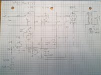
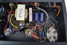
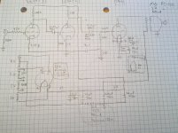
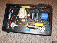
I've attempted to reverse-engineer the Mono 8 300B schematic based on pics from a recent eBay sale. Attached here is my first completed drawing, which is admittedly a little janky. I will make a better one with any corrections that need to be made, so I'd appreciate it if any interested members would like to check it over or point out any glaring errors.
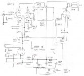
The topology differs slightly from the WPA 3.5 but uses many of the same values. The signal section topology is somewhat similar to the Fi Primer 300B in that signal input to the 300B grid is taken from plate 2 of the 6SN7 rather than cathode 2, though the power supply is quite different.
Like the WPA 3.5 (2A3), the Mono 8 uses a 10H/100mA/195R choke (the Hammond 158M) in the negative leg of the PS. The B+ rail seems to be taken from the first PS cap, while the 6SN7 plate supplies are taken from the third PS cap.
The two amps in the eBay sale had some differently branded capacitors and resistors, and apparently two different PTs. It seems one was repaired at some point. Of course it is possible that both amps were altered at some point in their lives (they bear serial #s 123L and 123R, with date code RIRH, and apparently assembled by George Wright himself).
Notes:
* Resistor stripe colors are not always clear in the pics, so some values may be wrong
* The second PS cap with the larger 220uf value is a screw terminal type mounted on top of the chassis. Seen from beneath the chassis, its terminals are obscured by other items in the PS, so I've made my best guess as to the topology there, but it seems largely to follow the WPA 3.5 (which uses a 100uf cap there).
* The light blue Xicon cap that parallels the 750R 10W coffin resistor has no values showing in the pics, though the same color and brand of cap is used in the WPA3.5 with values 100R 100V. It might be the same one but it is not possible to know without confirmation.
* The value of the hum pot is not visible, but the Xicon 750R resistor and by (100u?) bypass cap seem to act as the cathode array of the 300B. A 50R pot would make the effective cathode resistance 800R, while a 100R pot would make it 850R. Does either of these seem more likely -- or perhaps something else?
* The Xicon 750R resistor and bypass cap also seem to act as path to ground for the 680R resistors coming off the 6SN7 heaters.
* I have no idea what values are carried by the two red capacitors on the 6SN7: the little one from plate 1 (pin 5) to grid 2 (pin 1) and the larger coupling cap from cathode 2 (pin 3) to the 1.2K (?) grid leak resistor at the 300B grid. 0.22uF seems to be a common value for coupling caps to the 300B, but again I have no idea here. Maybe a simulation in LTSpice would net some possible operating points that would suggest a cap value there.
* There is a small silvery-blue cap with "F1" on the label which I've seen in a lot of George's amps. Any idea what brand and value that is?
* There is a small white axial component that looks like a diode in size but would more likely (I think) be a bypass cap for cathode 2 (pin 3) of the 6SN7. There seems to be "120" on the label. Any idea what that is?
Attached are my drawing, a known good WPA 3.5 schematic for comparison, and a couple of the amp pics I used.
Attachments
Last edited:
Thank you Ketje for you suggestions back in June, which corrected some of my resistor value errors. Sorry I didn't respond then.
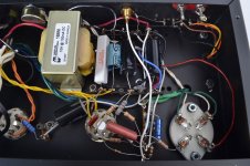
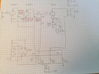
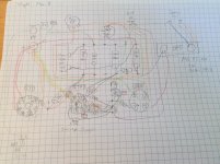
I've taken another go at it this morning using the interior pics attached in post #2. Attached here are my drawing of the circuit as it's layed out and my new attempt at a schematic.
I'd appreciate it if anyone could suggest or help identify possible values for the following components in the 6SN7 section (see red squared areas in drawing/schematic and the pics in post #2):
* Small red coupling cap from plate 1 to grid 2 (pins 5 —> 1)
* Second cathode (pin 3) resistor and little white bypass cap
(common values here are usually 23K-30K and 47uF 160V)
* Silvery-blue “F1" cap in the ground leg (possibly 0.47uF)
(it connects between the 270K and 75K resistors that go to the ground leg of the first [rightmost] 22uF/450V PS cap)
Maybe you've seen some of those before and know what they are?
Thanks!
Attachments
Last edited:
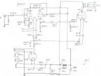
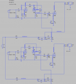
An owner of the Mono 8 with the 6DN7 input/driver tube (ca. 2001) was kind enough to send me some very good pics, from which I could derive a schematic (attached). The topology is nearly identical as the 6SN7 version, except there are no cathode bypass caps on the 6DN7, but at least we know all the part values.
I'm still stumped by that 750R cathode resistor on the 300B. It would require a really low operating voltage (ca. 250Vak -- resulting in only 4W output power) to stay within the 60mA spec for the FS-030 OPTs.
I wonder if George had the FS-030s airgapped for the 70mA range, which would allow for closer to 300Vak and the 7-8W output he claimed.
I just feel like I'm missing something here, as I've never seen a 300B SET designed like this before.
Attachments
FWIW, I have a couple of unfinished Mono 7 chassis and they have 820R 15W resistors.
Good luck finding your info.
I also found this product description for the Mono 7 on the web which might help explain the operating point choice. Possibly trying to make is sound more like the 2A3 is a partial explanation.
Product Description
The Mono 7 was designed to provide amplification for high SPL types of speakers while being both very low hum and noise while staying sonically pure. While the WPA3.5 Mono is a great amplifier, the Mono 7 at seven watts provides the power needed for a fuller performance. The seven uses a 300B but is designed to sound more like the 2A3 with the great mid range detail.
John
Thanks John. I agree. Tonight I received pics from inside the other Mono 8 and learned that the power transformer is labeled DMI 500-7694 0050, which Google tells me was also used on the WPA 3.5 and was manufactured by DeYoung. I've written them to ask for specs, but this suggests that the Mono 8 might have run at or near 2A3 voltages.
It's also possible that George had one transformer made for multiple amps, and that there's a higher voltage secondary winding for the Mono 8, but we'll see.
Btw, I tried to map the Mono 7 circuit but don't have good enough pics. I can see, though, that it uses the same topology as the WPA 3.5, which has an extra bias resistor on the first half of the 6SN7 and takes the signal from the second cathode rather than the second plate, but uses DC heating on the 300B.
Right now on the breadboard I'm running what I guess you could call a kind of AC-heated Mono 7 (schematic attached). It's the front end of the WPA 3.5 with a 300B output stage, but run at a very different operating point (350Vak, 1.5K cathode resistor, and 50mA plate current), and in a stereo build with one 5U4GB rectifier into a split rail power supply. It sounds fantastic but not quite the same character as George's stuff.
Correction to the schematic in post #5 -- the 6DN7 2nd plate load resistor is 270 ohm, not 170 ohm.
Attachments
Last edited:
In post #4's schematic, it seems to be using back-bias (see post #3) combined with the 750R cathode self-bias. Post 5's schematic likely contains an error - the 27k (from the 200k at the 300B's grid) should be connected to the choke like in post #4 and not to ground as shown.
..........
V3 neg needs to go to L6 , not GND directly
V3 neg needs to go to L6 , not GND directly
So you're saying the negative leg of V3 can accurately stand in for the center tap of the PT's high voltage winding?
I didn't inlcude the PT and rectifier tube because I haven't figured out how to get that working well. I've made one, but the simulation never registered the DC voltages after the rectifier tube and it took several hours to render a transient analysis of just a few seconds.
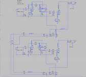
I did what you suggested and it lowered the B+ and 300B plate voltage by 10V, but maybe this is more accurate for the model's sake? Pic attached.
Attachments
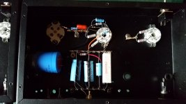
I took a photo of the underside of one of my incomplete Mono 7's. Hope it has something useful.
Thanks! What's the story behind these incomplete amps?
In post #4's schematic, it seems to be using back-bias (see post #3) combined with the 750R cathode self-bias. Post 5's schematic likely contains an error - the 27k (from the 200k at the 300B's grid) should be connected to the choke like in post #4 and not to ground as shown.
OK, so I felt conflicted about how to render the complexities of the actual circuit with the demands for simplicity of the schematic. I figured that the 27K resistor, for instance, ultimately went to ground, so I included the ground symbol, but then added a light dotted line to show where it connects in the negative leg of the PS. It was an attempt to provide all the information, but it probably just ends up being more confusing.
The other connections that have come up in this thread are similarly noted with dotted lines.
Maybe a different schematic layout would be better, since so many downstream components connect back to the power supply. I've seen others where the PS and signal sections are mirrored off a single ground line (i.e. the PS would look upside down), so I'll try that.
So you're saying the negative leg of V3 can accurately stand in for the center tap of the PT's high voltage winding?
I didn't inlcude the PT and rectifier tube because I haven't figured out how to get that working well. I've made one, but the simulation never registered the DC voltages after the rectifier tube and it took several hours to render a transient analysis of just a few seconds.
I did what you suggested and it lowered the B+ and 300B plate voltage by 10V, but maybe this is more accurate for the model's sake? Pic attached.
that is , according to schematic in post #5
known practice - choke in GND route , so main GND is practically post choke
Obviously the schematic has to match the actual circuit design. The back bias also address your question on why the 750R cathode resistor was used unlike Wright's other schematics.OK, so I felt conflicted about how to render the complexities of the actual circuit with the demands for simplicity of the schematic.
that is , according to schematic in post #5
known practice - choke in GND route , so main GND is practically post choke
In that case, the signal section is wrong too, because the 6SN7 cathode resistors connect to the choke in the negative leg as well. I didn't make that connection on the breadboard either, so the actual amp is wrong too. I mean, it works and sounds good, but it doesn't have the back-bias that the WPA 3.5 has.
Thanks for pointing out these errors. Still so many newbie mistakes.
Obviously the schematic has to match the actual circuit design. The back bias also address your question on why the 750R cathode resistor was used unlike Wright's other schematics.
He uses the 750R in both the WPA 3.5 and the Mono 8, though the incomplete Mono 7 we've been shown has an 820R.
The other Mono 7 pics I have show a heavy duty wirewound resistor mounted to the chassis, but I can't read the value printed on it. Could be 820R like in nerdorama's.
Attachments
So where does the 1.5k in the LTSpice sim come from?
Sorry for this, but it's kind of a long story. My friend owned a pair of Mono 8s with the Magnequest TFA-204 OPTs rather than the FS-030 that it came with. We are trying to re-create them because he had to sell them back in 2004. So I'm trying to accurately map the Mono 8 circuit as a starting point and then figure out if changes would need to be made for use with the TFA-204.
The 1.5K thing is from the first part of this journey, when my friend thought he had owned a pair of WPA 3.5 modified by George to have a 300B output section (before a search of his old emails revealed he'd actually ordered the modified Mono 8). His amps were in the WPA 3.5 chassis because it was already drilled for the TFA-204 (suggesting the PT was the same in both models), but had the Mono 8 circuit inside. That was before I saw inside the Mono 8, and wouldn't have imagined that 300B had the same cathode resistor value as the 2A3 amp.
Anyway... since I thought I was starting with the WPA 3.5, I had to use a combination of evidence and speculation to try and figure out what the 300B stage might have looked like. I assumed that George would have used a traditional operating point for the 300B, like 350Vak/60mA (the TFA-204's DC current rating) into a 3K load, as per the Western Electric op point table. That would dictate a ~1.2K cathode resistor (or so I thought).
However, since I'm trying this out on a breadboard with parts I have on hand, and my only OPTs are a pair of Electra-Print 5K:8ohm from an earlier project, I picked the WE op point of 350Vak/50mA into a 5K load, which requires a 1.5K resistor to get there.
The idea was to get it close on the breadboard before moving on to a fully accurate final build down the road.
BUT...
I have recently realized that the load impedance is not simply the AC impedance of the OPT primary winding but is *reflected* from the speaker's impedance curve through the secondary and primary of the OPT.
So, I'm not doing what I thought I was and you get to watch me make all the newbie mistakes. I have impedance curves measured by someone else for the speakers I have (JM Lab Electra 905) but haven't had time to figure it out and work with the breadboard recently because we bought a puppy at the horse track on Saturday night and she has turned our lives upside down.
Hence, I've devoted my energies to figuring out the Mono 8 before trying anything else.
Last edited:
In that case, the signal section is wrong too, because the 6SN7 cathode resistors connect to the choke in the negative leg as well. I didn't make that connection on the breadboard either, so the actual amp is wrong too. I mean, it works and sounds good, but it doesn't have the back-bias that the WPA 3.5 has.
Thanks for pointing out these errors. Still so many newbie mistakes.
nope .......
everything in circuit is connected to one - main audio GND
fact is "just" that audio gnd is established not on CT of xformer , but after choke
in sim - neg leg of power supply is same thing as CT of power xformer
so , choke from there , then GND symbol
- Status
- This old topic is closed. If you want to reopen this topic, contact a moderator using the "Report Post" button.
- Home
- Amplifiers
- Tubes / Valves
- Wright Mono 8 Schematic & Operating Points