Hi,
I have started a small SMPS design with Power Intergrations circuits using aTinySwitch II Series IC.
My design is similar to "Engineering Prototype Report 14" except for the output voltage being 4,1 V/1,2 A instead of 9 V/0,3 mA and it also uses a TL431 shuntregulator instead of the zener used in their schematics to regulate output voltage seen in EPR 14 document on page 5.
The prototype started up fine and with 4,09 V at output with a 1 kohm bleader resistor on the output not leaving the output unloaded.
My problem is that the output voltage changes too much with load not expected by me with a shunregulator, max output current is around 1,2 A and at full load the output voltage is only 3,7 V, decreased with 0,4 V which is unacceptable for me, 0,1 V would be the target.
The configuration with the TL431 is the same as in Powerintergrations EPR 29 seen on page 5.
One problem is of course the HF ringing occuring at switch-off which becomes repeated much more often with increasing load.
Unfortunately I have at my hand only a 20 MHz scope and another problem is the continuosly modulating switcing frequency which makes it hard to inspect the curve traces.
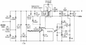
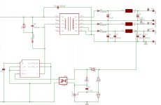
BTW, I made up quickly with MSpaint copy-paste from both schemativs in above mentioned PDF's which looks like my PSU which I will try to attach here below.
Suggestions?
Thoughts regarding TL431 and high frequency disturbans?
Michael
I have started a small SMPS design with Power Intergrations circuits using aTinySwitch II Series IC.
My design is similar to "Engineering Prototype Report 14" except for the output voltage being 4,1 V/1,2 A instead of 9 V/0,3 mA and it also uses a TL431 shuntregulator instead of the zener used in their schematics to regulate output voltage seen in EPR 14 document on page 5.
The prototype started up fine and with 4,09 V at output with a 1 kohm bleader resistor on the output not leaving the output unloaded.
My problem is that the output voltage changes too much with load not expected by me with a shunregulator, max output current is around 1,2 A and at full load the output voltage is only 3,7 V, decreased with 0,4 V which is unacceptable for me, 0,1 V would be the target.
The configuration with the TL431 is the same as in Powerintergrations EPR 29 seen on page 5.
One problem is of course the HF ringing occuring at switch-off which becomes repeated much more often with increasing load.
Unfortunately I have at my hand only a 20 MHz scope and another problem is the continuosly modulating switcing frequency which makes it hard to inspect the curve traces.
BTW, I made up quickly with MSpaint copy-paste from both schemativs in above mentioned PDF's which looks like my PSU which I will try to attach here below.
Suggestions?
Thoughts regarding TL431 and high frequency disturbans?
Michael
Attachments
Are you ensuring proper TL431 biasing by placing a 470 ohm resistor in paralell with the led of the optocoupler?
Note that the feedback current the phototransistor is required to draw from the tinyswitch is only approx. 250uA while the TL431 requires more than 1mA for optimum biasing.
Also, be aware of placing any capacitance between A and K pins of TL431 because it may oscillate. The datasheet includes a graph showing valid capacitance values for different 'gain settings'.
Hi Eva,
who else then you would appear to help a guy with SMPS design issues!")
I should say it again that the schematic is an approximate copy of my SMPS, I didn't take time to draw it up in a schematic editor so I just copy pasted from PI's two diffrent paper just for this post here on DIYaudio, as explained in my first post, lazy me.
The values differ just slightly so it's quite accurate.
The PC817A LED has an 1 kohm in paralell, I meassured the series resistor R9 to have a voltagefall corresponding to 1,5 mA and should be sufficient.
But maybe I will try to lower the value a bit.
The Capacitor in paralell with TL431 is from Power Intergrations EPR 29 paper, it's 10 uF electrolytic capacitor and PI explains this with giving the SMPS a softer start as it draws more current through the LED at charge up.
But I insist with out, it amazed me too a bit before I saw their explanation, actually the SMPS don't oscillate.
I have to say it again, these all-in-one el-cheapo circuits is a h*ll to work with because of their modulated switching frequency if using a modest oscilloscope, and scopes are necessary when developing SMPS's...
My theory is that it has too much HF ripple which the shunt reg cant handle every time the primary switches off, we are talking about MHz ringing.
So, when the load is increasing, the Tiny will increase the train of switching pulses (or how I should explain that as it has some type of "switch skipping" scheme) or should i say decreasing the skipping rate by load so the HF ringing will be more frequent and thereby the shunt reg can't notice the actual voltage as it contains more DC-overstored HF energy exceeding the stable charge voltage in the electrolytes seen between the switching moments...?
Anyhow, I suspect strongly the HF energy is affecting on the shunt reg in some way and have also considered a redesign of the PCB layout even if in current design I have already located the feedback circuitry couple of cm from the transformer because where they are now I could have located these components even much closer because of the free space.
Actually I even made a "dead" strip on the PCB layout between transformer and feedback circuitry connected to the transformers return/GND in an attempt to lower the stray pickup a bit.
Michael
who else then you would appear to help a guy with SMPS design issues!
I should say it again that the schematic is an approximate copy of my SMPS, I didn't take time to draw it up in a schematic editor so I just copy pasted from PI's two diffrent paper just for this post here on DIYaudio, as explained in my first post, lazy me.
The values differ just slightly so it's quite accurate.
The PC817A LED has an 1 kohm in paralell, I meassured the series resistor R9 to have a voltagefall corresponding to 1,5 mA and should be sufficient.
But maybe I will try to lower the value a bit.
The Capacitor in paralell with TL431 is from Power Intergrations EPR 29 paper, it's 10 uF electrolytic capacitor and PI explains this with giving the SMPS a softer start as it draws more current through the LED at charge up.
But I insist with out, it amazed me too a bit before I saw their explanation, actually the SMPS don't oscillate.
I have to say it again, these all-in-one el-cheapo circuits is a h*ll to work with because of their modulated switching frequency if using a modest oscilloscope, and scopes are necessary when developing SMPS's...
My theory is that it has too much HF ripple which the shunt reg cant handle every time the primary switches off, we are talking about MHz ringing.
So, when the load is increasing, the Tiny will increase the train of switching pulses (or how I should explain that as it has some type of "switch skipping" scheme) or should i say decreasing the skipping rate by load so the HF ringing will be more frequent and thereby the shunt reg can't notice the actual voltage as it contains more DC-overstored HF energy exceeding the stable charge voltage in the electrolytes seen between the switching moments...?
Anyhow, I suspect strongly the HF energy is affecting on the shunt reg in some way and have also considered a redesign of the PCB layout even if in current design I have already located the feedback circuitry couple of cm from the transformer because where they are now I could have located these components even much closer because of the free space.
Actually I even made a "dead" strip on the PCB layout between transformer and feedback circuitry connected to the transformers return/GND in an attempt to lower the stray pickup a bit.
Michael
There are several things I would measure in order to understand such a problem:
- Voltage waveform at TL431 gate pin.
- Voltage waveform before and after the smoothing inductor.
- Voltage at TL431 cathode, is it saturating? it should have 2.5V or more between K and A.
Ummh... Now that I've mentioned it...
Your photodiode is dropping approx. 1.5V (1.5mA@1Kohm) and the current limiting resistor placed in series with it is also dropping some hundreds of milivolts, so Vka of your TL431 is probably lower than 2.5V. With such a low voltage it's not likely to work properly, namely the Vref may be no longer 2.5V but lower.
I would try to temporarily increase output voltage to 5V. Don't panic if this is the cause of the problem, I've already figured out some posible solutions.
PD: I neither like these compact ICs, I developed my own self oscillating flyback for low power applications:
http://eva.eslamejor.com/aux10w_0.jpg
http://eva.eslamejor.com/aux10w_1.jpg
http://eva.eslamejor.com/aux10w_2.jpg
Jackinnj,
I ordered a ready made transformer from a manufacturer who claimed they make transformers for TNY circuits normaly.
The spcification I have at my hand says
* 2300 uH for primary
* leakage 13 uH
(they meassured it)
I have already EFD transformer kit but when i got this ready made transformer i didn't start to calculate the transformer.
One annoying thing seem to be that they have used cores without airgap, so they added some thin paper between or so, too bad if so because the stray magnetic field is worser for surrounding components...
Eva,
I have meassured and made some changes and tests now for couple of hours, I even made a voltage doubler just for feeding the optocoupler and I got between 10-20 V depending on load an input voltage, unfortunately it didn't help much.
I noticed that the output voltge is very stable with changing input voltage from 85 to 250 VAC(Actually I should go to 265 VAC but the variac didn't do it), at no load to almost full load the output is changing only some 10 mV with changing mains voltage, very nice.
This gives me a clue that it might be the HF energy that interfer somehow with the TL431 as the Tiny switches more frequent by load, so I have started to think if I can "rectify" that HF energy and "backfeeding" it to the shunregulator circuitry at some node and fool it so it will compensate.
Well, right now I'm pretty tired so I have to rest a bit.
BTW funny that your SMPS in your picture attached looked a lot like mine, I will post later some pictures.
A note: I should mention and make it clear that 4,1 V/1,2 A is not really full load but the mean load and should momentarily supply upto 2 A as the circuit the SMPS going to feed draws short pulses up to 2 A, but mean load is about 1,2 A. So I have to chose a balance between bulky el-lyte's or capable transformer.
Michael
I would HIGHLY suggest to get rid of the PI part and get a ST micro part .....
I have had it out many times with PI, they are arogant and think they are experts in switching supplies...
My job in one company was to redesign and improve the PI designs...
What are the output specs for the supply you would like to have?????
Majority of the problems like you describe are usually a result of the loop compensation.... The TL431 with an Opto is SLOW and low frequency POLE usually down about 8K to 10K at best....
Did you account for the worst case CTR of the OPTO????
The inductor size seems a bit odd..... Not to worry about the gap...Your main concern is adjusting the VOR and peak current to where you want them figuring the inductance last....the GAP will take care of itself if you design the transformer properly...
The Y cap is also a major issue here and is a HUGE current leakage.... It is there for EMI reduction, since returning it to the BUSS... But if you do not need to comply to standards , do not use it....
Chris
cerrem said:I would HIGHLY suggest to get rid of the PI part and get a ST micro part .....
I have had it out many times with PI, they are arogant and think they are experts in switching supplies...
My job in one company was to redesign and improve the PI designs...
What are the output specs for the supply you would like to have?????
Majority of the problems like you describe are usually a result of the loop compensation.... The TL431 with an Opto is SLOW and low frequency POLE usually down about 8K to 10K at best....
Did you account for the worst case CTR of the OPTO????
The inductor size seems a bit odd..... Not to worry about the gap...Your main concern is adjusting the VOR and peak current to where you want them figuring the inductance last....the GAP will take care of itself if you design the transformer properly...
The Y cap is also a major issue here and is a HUGE current leakage.... It is there for EMI reduction, since returning it to the BUSS... But if you do not need to comply to standards , do not use it....
Chris
I ran the trafo inductors in POWER456 and it was "high" but not out of the realm of reasonable.
I am guessing this is a 300kHz supply.
I am not even going to guess -- but there should be a 1nF/470R snubber across the secondary diode.
I will run the loop comp in 456 tomorrow, but I don't think that this is the problem.
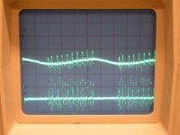
Ultima Thule said:...and finally a oscilloscope picture.
The above wave trace is outputvoltage, settings are 20uS/div resp. 200mV/div.
Below is the voltage seen at the shunt regs ref input, 10mV/div
Michael
It seems that your circuit is oscillating at 8.3Khz (120uS period), otherwise it would reach a steady state, even though the IC uses variable frequency.
Note that flybacks with multiple outputs are evil. That self oscillating flyback you have seen gave me some headaches due to stability issues. I suggest temporarily removing the flyback diodes from the unused outputs.
A basic understanding of how Tinyswitch works will help explain some of what is going on. It is not your standard PWM controller, but drops out pulses depending on state of the enable pin in order to achieve output regulation. TinySwitch I has a fixed current limit, while TinySwithch II has a state machine inside that shifts to several discrete current limit steps depending on the previous state of the enable pin. This is explained n the data sheets. Because of this feature, the output ripple will look funny compared to a standard PWM controller. Despite this, it's not too hard to work with if the transformer is OK and you follow a few basic rules. If the transformer is poorly designed, it will be hard to get decent results with anybody's chip.
I generally do not trust pre-made transformers at all for my switching power supply designs, unless I can reverse engineer the and be satisfied with what I see. Instead, I design and wind the first prototypes myself. You don't need a lot of kit to make prototype transformers, as long as you have access to the cores and bobbins. I started out long ago putting the transformer bobbins on mandrels carved from pencils and wound everythng by hand. Very ugly, very clunky, but it worked. If you have a better setup, of course it's a lot easier. It is good to have the actual polyester film tape used in transformer manufacture, but ordinary tape will get you going for a first unit (that unit should stay in house, though). You can shim gap with tape, mylar film or paper. If the gap is large enough, you can grind it using a hand tool ("Dremel") and an abraisive drum. This is very rough and ready, but you will get results. The shim gap will be more consistent than a hand ground gap. If the gap isn't very big, you shouldn't have much of a problem with fringing flux, and you can put a flux band around the transformer with copper foil that will halp reduce this. The EFD series of cores is not a favorite series of mine for AC-DC work, as they were designed for low profile DC-DC converters and it is fairly hard to make a transformer without flying leads that will meet safety rules, except for the larger cores in the series. If you are trying to get a prototype going and that's all you have, they can be made to function.
In my experience (and many of my customers), if you give a transformer manufacturer free rein with a transformer design, you will often get a Frankenstein monster that works poorly. Typical problems can be excessive winding capacitance, core saturation at startup or heavy loads, poor load and cross regulation. Transformer manufacturers are very good at making transformers in large quantities according to specs that you give them ( it's their business, after all), but not necessarily so good at designing switching power supplies. There's always exceptions to this, but I don't see them very often. Since the transformer is the very heart of a flyback supply, you can understand the importance of making sure that the transformer vendor has his act in gear, and in keeping control of that part of the design. It is a good idea to download the PIXLS spreadsheet program and use it to reverse engineer the transformer design, if you can get the vendor to give the number of turns in the windings. It's also a useful too to desighn your own stuff.
Having said this, though, I don't necessarily think that the transformer is the problem. The ripple waveform shows a lot of pulse bunching. At the power supply switching frequency, the TL431 should be compensated so that it is essentially standing still and not trying to respond to any high frequency signal. At high frequencies, a well-compensated TL431 will look like a zener diode, and switching frequency signals will propogate right through from cathode to anode. It is a seconf HF feedback loop in addition to the formed by the output voltage divider and reference pin. This is something not generally understood, and can cause a lot of confusion when you are trying to measure gain /phase on a supply using a TL431 supply. Breaking the control loop at the output voltage divider only gets you a piece of the loop, and generallly not the piece that will cause you problems.
It is the HF ripple signal propogating through the optocoupler and TL431 cathode that actually makes the enable signal on the Tinyswitch go when it should. The TL431 cannot slew fast enough to make it happen, and you don't want it to try. If the TL431 is wallowing around or oscillating (they will half-heartedly try to respond to high frequency signals, including stray RF fields), this can show up as poor load load regulation. This isn't unique at all to PI stuff - I've also seen iit happen with a UC3842-based supply.
I generally use a default compensation network of 100nF and 3k3 when starting a Tinyswitch design, and I rarely have to change it.
The next step is to choose a good value for the resistor in series with the optocoupler input LED. A value of 470 ohms is a good starting choice for a 5V output and an opto like the PC817A with 80-160 CTR. Since your output voltge is lower, you may want to start with 470 ohms, than maybe move down a bit.
The other two important bits that are germane for any switching power supply design, but also important here, are to have a tight secondary layout and good quality output filter caps in the first stage after the output rectifier. For normal size electrolytic caps used in switcher outputs, the HF ripple waveform will consist almost entirely of the product of the capacitor ripple current with the capacitor ESR, along with HF trash at ther edges due to stray inductance. If the ripple signal is too large due to high ESR, you can swamp the TL431/opto system, and your load regulation will suffer, as the controller cannot respond properly. Again, this can happen with other controllers as well as PI stuff, but it is more important for the Tiny, as it is getting information from the ripple. If the capacitor ESR and ripple current rating are chosen to line up with the output current (just like any other flyback design), it should work just fine. You don't need a super-duper high quality cap, but it sould be rated for switcher duty. Something on the order of a Panasonic HFQ (which is mediocre these days) will be ok. If you aven't heard this, you should know as a rule of thumb that the ripple current in the output caps of a flyback supply will be on the order of the output current.
Look at it this way - for the voltage to remain the same at the power supply output, the current coming out of the filter cap when the primary switch is on and the output rectifier is reverse biased is equal to the output current, assuming the ripple is small compared to the output voltage. When the primary switch turns off and the output rectifier turns on, the secondary must restore the charge lost from the output cap and deliver the output load current in order to keep the output voltage constant. If you have a perfect flyback with infinite primary inductance, the tops of the waveform will be flat, and you get a quasi-square wave of current through the output cap. At 50% duty cycle, the RMS value is equal to the peak, so the RMS ripple current in the cap is equal to the output current. In a real-life situation with waveform tilt, you actually get 20-30% more ripple current, but the simple-minded assumption gets you in the ballpark for a first-cut prototype.
If the loop consisting of the transformer, output rectifier and first filter cap is too large, you can add a lot of stray inductance, which shows up on the output ripple, and can also degrade cross regualtion. This stray inductace also gets reflected back to the primary multiplied by the square of the turns ratio, and looks like extra leakage.
I hope some of this extended screed is useful to you. If it's any encouragement, I built up a 5W, 5V TinyII design with TL431 output sense just last week, rolling my own transformer and following the basic rules I just discussed. Once I got my own little dummheits straightened out (open solder joint), it took off and ran with almost perfect load regulation (perfect according to the DVM).
Hi, and many thanks to all for your professional help!
The manufacturer I used for the transformer mentioned is PCA Electronics inc., my first thought was.. "is this going to work as a Forward...".
I thought too the inductance looked to be too high.
I going to be short this time, dont have time to write much just now but will uppload a schematics with some values on the components used.
The parallel resistor with the optocoupler, I have tried 1kohm and 500 ohm(2//1kohm).
El-lytes are low ESR 105 C suggested for SMPS use.
Anyhow I will start to design my own transformer right now, I have EFD 15, 20 and 25 and will start with EFD 20.
(Theres no problem with isolation as I'm going to use tripple insulated wire (and Polyester tape too of course)later on and thereby don't have to fullfill large clearance and creapage distances which use to be a pitfall for small core dimensions in general that are supposed to work with mains voltages.)
But more to come later.
Michael
Attachments
These are the winding notes I took for my flyback transformer:
----------------------------------------------------------------------
my requirements:
primary 15V --> aux 500mV --> secondary 720mV
ratio 30:1 [aux] and 21:1 [secondaries]
primary inductance: 3.3mH up to 500mA, >400uJ
filter : 470u + 6.8u@3A + 470u for each output
actual transformer:
primary : 42+42T + 42+42T --> between 3.6mH and 4mH and >500mA saturation, >600uJ measured
Vreflected=88V, pin 11* 10
s1=25T --> 12V pin 6* 7 (single layer)
s3=72T --> 36V pin 4* 5 (two layers)
s2=40T --> 20V pin 2* 3 (single layer)
fback : 8T, pin 12* 9 (single layer, self oscillating feedback)
layout: (inner) pri1 : pri2 ::: s2 : s31 : s32 : s1 ::: pri3 : pri4 : fback (outer)
note: ':' means a layer of mylar tape
note: the coil former only allows for up to 42 turns per layer
----------------------------------------------------------------------
Cores were two E20/10/6 halves of N27 material with 0,17mm built-in center-leg gap each, from EPCOS (Germany). Wire had 0,22mm for all windings
I also bought some EFD cores and tested them, but they showed very poor energy storage abilities so I discarded them for flyback applications.
I hope you may find this useful.
----------------------------------------------------------------------
my requirements:
primary 15V --> aux 500mV --> secondary 720mV
ratio 30:1 [aux] and 21:1 [secondaries]
primary inductance: 3.3mH up to 500mA, >400uJ
filter : 470u + 6.8u@3A + 470u for each output
actual transformer:
primary : 42+42T + 42+42T --> between 3.6mH and 4mH and >500mA saturation, >600uJ measured
Vreflected=88V, pin 11* 10
s1=25T --> 12V pin 6* 7 (single layer)
s3=72T --> 36V pin 4* 5 (two layers)
s2=40T --> 20V pin 2* 3 (single layer)
fback : 8T, pin 12* 9 (single layer, self oscillating feedback)
layout: (inner) pri1 : pri2 ::: s2 : s31 : s32 : s1 ::: pri3 : pri4 : fback (outer)
note: ':' means a layer of mylar tape
note: the coil former only allows for up to 42 turns per layer
----------------------------------------------------------------------
Cores were two E20/10/6 halves of N27 material with 0,17mm built-in center-leg gap each, from EPCOS (Germany). Wire had 0,22mm for all windings
I also bought some EFD cores and tested them, but they showed very poor energy storage abilities so I discarded them for flyback applications.
I hope you may find this useful.
I have downloaded https://www.onsemi.com/site/survey/ONPowerDesigner.zip this from ONSemi. This is a Fly-Back SMPS designer. The feedback is made with TL431+optocoupler.
Can I use this xls file to design the feedback to a push-pull current mode SMPS ?
Can I use this xls file to design the feedback to a push-pull current mode SMPS ?
On using the EFD cores for line input SMPS - with the usual stock bobbins available for the EFD series, using triple insulated wire is not sufficient for primary-secondary isolation. A tape margin is needed on the side next to the secondary pins to get the required creepage from primary winding to secondary pins. Primary pins to core to secondary pins will be aniother problematic leakage path requiring one to tape wrap the cores. Power ferrites are quite, quite conductive at mains voltages. No joke at all - I've been burned in this manner with other cores and bobbins. Custom bobbins can be tooled to get around the leakage problems, but most people are not willing to do this unless the run rate is sufficiently large.
I agree with Eva - EFDs don't give you much power capability for the amount of space they hog on the board. Still, they tend to be used where component height is a major concern, such as internal supplies for LCD monitors. For the particular application in question here, an EE or EF16 would probably suffice, but getting the proper bobbin to meet safety could be a chore, as they are all made in Taiwan, China, HK, or Korea.
I agree with Eva - EFDs don't give you much power capability for the amount of space they hog on the board. Still, they tend to be used where component height is a major concern, such as internal supplies for LCD monitors. For the particular application in question here, an EE or EF16 would probably suffice, but getting the proper bobbin to meet safety could be a chore, as they are all made in Taiwan, China, HK, or Korea.
Wrenchone (whats your name btw?)
thansk for attracting my attention to those issues you mentioned with EFD, I have parts from ferroxcube and will check up that closer.
I have 3F3 I will try out.
I am aware of some ferrite being quite conductive, I once touched with the oscilloscope probes earth a bead (I think it was 3S1) which was after the Booster, eg. around 380-400 Volts, and yes I experienced some flashes.
Thanks Eva for your input!
Does anybody have experiences with planar cores and PCB windings operated from the mains, or some Payton with their special coilformers?
Just asking of curiosity, I'm not forced by low profile building height and can use EE, EC or similar shapes too.
Michael
Why would you want to torture yourself with a planar transformer design unless you really need one? They are generally only useful for lov voltage DC to DC designs at relatively high freqencies. These applications are usually about the only ones where it would be worth the extra expense and bother. I speak of course from the perspective of an inexpensive, high run rate design. It may be different for military/aerospace applications.
- Status
- This old topic is closed. If you want to reopen this topic, contact a moderator using the "Report Post" button.
- Home
- Amplifiers
- Power Supplies
- Problem with TL431 in a SMPS