I had all of the -ve side connections just along a strip from load back to the diode bridge. This is not good as there is shared current seen.
This seems to be what I have. Not completely sure I'm clear on what you mean by "shared current seen". An example?
BTW I've did a bit of reworking of the layout yesterday based on input and will look how I might further incorporate several of your recommends. Don't want to post every version as I go! Thank you for the specific recommends along with the reasoning behind them.
Ideally the adj cap and 1.12K resistors should connect direct to the load (ie the zero volts point for positive and the -ve output for the negative) and not back along the strip (as is most convenient).
Not really sure how I could connect these directly when there are two caps & and LED in between... and one a fat film cap.
And then again...
- If my maths are right, a standard strip is 2mm x 35um which comes to 0.07mm2.
- Standard hookup wire is 22AWG or 32mm2.
- Beefier 20AWG hookup wire is 52mm2.
Since PCB traces often aren't much more, it seems the way PCB-based PSU boards handle this is by maximizing the size and continuity of a ground plane.
So a strip ain't much! It would take nearly 5 strips joined along their length to equal standard hookup wire... or just a second strip with a bare 20AWG wire soldered directly along it's length to do much better.
Last edited:
I suspect (but could be wrong) that the resistance of the trace for the adj connection (to the negative potential part of the circuit, as opposed to the output of the reg), is not critical. I think it is more about making sure it is seeing only the load current.
If you tap in along the trace, you also have any noise current that has gone through the filter caps on the output of the reg. That's the "shared" current I was talking about. You want it to be sensing JUST the load current.
Tony.
If you tap in along the trace, you also have any noise current that has gone through the filter caps on the output of the reg. That's the "shared" current I was talking about. You want it to be sensing JUST the load current.
Tony.
I read about that layout technique about twenty years ago....................
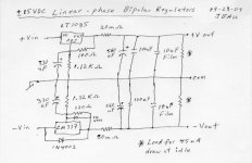
AndrewT offered me some advice on the layout (as I also did it on strip board and was unsure what was important) I had all of the -ve side connections just along a strip from load back to the diode bridge. This is not good as there is shared current seen. Ideally the adj cap and 1.12K resistors should connect direct to the load (ie the zero volts point for positive and the -ve output for the negative) and not back along the strip (as is most convenient).
The other one that is important is the connection of the top resistor (100 ohms) you should ideally connect it to the case of the regulator. I soldered mine directly to the out pin of the reg above the circuit board. See below from LT1086 datasheet.
Tony.
Then someone posted a link to a paper and it turned out to be that same one I read such a long time ago.
It really is important that low level current circuits do not share traces/wires with high level current circuits.
It is a development of that thought that brought me to realise that LOOP AREA of individual TWO WIRE circuits is what we need to strive for. Forming the TWO WIRE circuits becomes the first priority.
Wintermute's post19 sch shows the important LAYOUT considerations that are usually omitted from generalised sch that only show GND symbols.
Last edited:
I suspect (but could be wrong) that the resistance of the trace for the adj connection (to the negative potential part of the circuit, as opposed to the output of the reg), is not critical. I think it is more about making sure it is seeing only the load current.
If you tap in along the trace, you also have any noise current that has gone through the filter caps on the output of the reg. That's the "shared" current I was talking about. You want it to be sensing JUST the load current.
Tony.
If that were the case, couldn't one address it by leaving all the VE- connections intact (as in the layout PNG), but solder a bare 20AWG wire along the VE- strip, but only on the section between the adjust cap and the load? That way you are using one strip, but dramatically lowering the impedance (increase the sensed connection) between the adjust cap and load.
Or alternatively, connect the adjust cap and 1.2k resistor to a separate strip that connects to the load only at the end, and perhaps has a bare wire soldered along it to decrease impedance/increase sensed connection?
...we still have the distance between reg load created by the large film cap. Bares some thinking.
The other one that is important is the connection of the top resistor (100 ohms) you should ideally connect it to the case of the regulator. I soldered mine directly to the out pin of the reg above the circuit board. See below from LT1086 datasheet.
Tony.
With the adjust cap added, the schematics (datasheet or JBau's) might imply a certain order to the adjust loop (C-R2-R1). Does it matter whether I connect the 166R resistor much closer to the adjust pin rather than just after 1.2K resistor?
Attachments
I perhaps should have posted the text that went with the datasheet graphic I posted.
It always seemed odd to me that a difference of 0.05 ohms could make a difference when the resistor itself was 240 ohms but, I'm obviously missing something, however it didn't stop me from implementing as they suggested , although that is for an LM317 the same concept is mentioned in the LT1086 datasheet, and I would guess also the LT1085 one (actually the LT one appears to have a typo in it, but the LM1085 one from TI says pretty much the same thing)..
actual datasheet that came from http://www.jameco.com/Jameco/Products/ProdDS/898800.pdf
Tony.
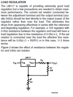
Actually there is some more info, but a better description is available in one of the LM317 datasheets... just found it, it is from one of the original National Semiconductor datasheets. see below:Although it may not be immediately obvious, best load regulation is obtained when the top of the resistor divider R1 is connected directly to the case not to the load, as illustrated in Figure 2.
It always seemed odd to me that a difference of 0.05 ohms could make a difference when the resistor itself was 240 ohms but, I'm obviously missing something, however it didn't stop me from implementing as they suggested
, although that is for an LM317 the same concept is mentioned in the LT1086 datasheet, and I would guess also the LT1085 one (actually the LT one appears to have a typo in it, but the LM1085 one from TI says pretty much the same thing).. actual datasheet that came from http://www.jameco.com/Jameco/Products/ProdDS/898800.pdf
Tony.
Attachments
Last edited:
There is no amplification in a power supply so RF is not a problem as there is nothing to upset by way of a tuned circuit/aerial.
If you decouple the supplies as per the data sheet; 10u Tant bead capacitors, you will have no problem but if you use higher value capacitors you will run into trouble not to mention extra cost.
If you have a regulator in the power supply, there is amplification. In fact there is an entire feedback loop to deal with.
Or alternatively, connect the adjust cap and 1.2k resistor to a separate strip that connects to the load only at the end, and perhaps has a bare wire soldered along it to decrease impedance/increase sensed connection?
I think that is what I did in the marked up layout I posted
unless I stuffed it up!! SANS the extra wire to reduce the impedance of the trace.. Tony.
Last edited:
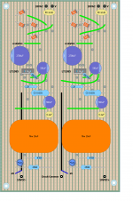
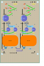
So here is the latest version layout (B), one possibility. I am assuming that the hookup wire is a lower impedance than the trace strips because it is 4.5x more copper. So hookup wire connections are even stronger electrically than strip connections... but that's without considering the role of solder joints!
Note that the black lines are bare wires soldered directly to the trace underneath. So the Adjust loop has it's own line to load that is separate from everything else's connection to load a couple strips away. And the Adjust load is a stronger pathway to load than others have. ...Not sure this was necessary ... could put similar copper wires along all four lines to load.
The two sides are not quite symmetrical, mostly to give room between VDC- and the adjacent standoff.
I also tried to keep a spare hole in between solder points on the same strip. This is mostly to keep solder joints distinct, and makes unsoldering/resoldering easier for me.
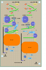
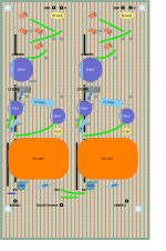
In case you want to see a couple variations, (BB) has two versions:
Note that the black lines are bare wires soldered directly to the trace underneath. So the Adjust loop has it's own line to load that is separate from everything else's connection to load a couple strips away. And the Adjust load is a stronger pathway to load than others have. ...Not sure this was necessary ... could put similar copper wires along all four lines to load.
The two sides are not quite symmetrical, mostly to give room between VDC- and the adjacent standoff.
I also tried to keep a spare hole in between solder points on the same strip. This is mostly to keep solder joints distinct, and makes unsoldering/resoldering easier for me.
In case you want to see a couple variations, (BB) has two versions:
- Right - with the connections to the Adjust pin a little different.
- Left - reworking all a bit to shorten the traces (strips) needed by about 25mm. Worth it?
Attachments
I happen to like Stripboard for quick builds, and I've invested a few dollars in CAD software that makes it even quicker and easier (link to diyAudio thread)
In my experience the most common failure mode is short-circuits between adjacent strips, due to tiny solder bridges. A headband magnifier with a light will usually reveal the culprit after a couple minutes of careful scrutiny. Best to "buzz out" the board with a continuity tester / beeper, before applying power the first time.
In my experience the most common failure mode is short-circuits between adjacent strips, due to tiny solder bridges. A headband magnifier with a light will usually reveal the culprit after a couple minutes of careful scrutiny. Best to "buzz out" the board with a continuity tester / beeper, before applying power the first time.
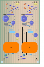
Hi Bruce, I wanted to look at those on my big monitor (but didn't get the chance). One thing I don't like about the space saving version is the positioning of the 560uF cap. Having long leads to BOTH of the pins of the cap I don't think is good (on the earth side ok, but not on the load side IMO). I could of course be completely wrong on this, but I don't think I've ever seen the output caps remote from the actual output trace.
It's probably being picky, but I'd also like to see the -VE link on the other side of the circuit common and 10V- output points on the board.
Tony.
It's probably being picky, but I'd also like to see the -VE link on the other side of the circuit common and 10V- output points on the board.
Tony.
I read about that layout technique about twenty years ago.
Then someone posted a link to a paper and it turned out to be that same one I read such a long time ago.
It really is important that low level current circuits do not share traces/wires with high level current circuits.
It is a development of that thought that brought me to realise that LOOP AREA of individual TWO WIRE circuits is what we need to strive for. Forming the TWO WIRE circuits becomes the first priority.
Wintermute's post19 sch shows the important LAYOUT considerations that are usually omitted from generalised sch that only show GND symbols.
I'm starting to see some of the elegance of Andrew's way of thinking about this and the multi-encompassing nature of it.
Hi Bruce, I wanted to look at those on my big monitor (but didn't get the chance). One thing I don't like about the space saving version is the positioning of the 560uF cap. Having long leads to BOTH of the pins of the cap I don't think is good (on the earth side ok, but not on the load side IMO). I could of course be completely wrong on this, but I don't think I've ever seen the output caps remote from the actual output trace.
It's probably being picky, but I'd also like to see the -VE link on the other side of the circuit common and 10V- output points on the board.
Tony.
Yeah, the shortened board was looking more and more like a false benefit. The Reg side of the circuit was not any shorter; that was a fiction facilitated by the angled 20mR cs resistor... and in fact was longer due to the position of the 560uF cap. It didn't really feel right, even though the shorter board gave the illusion of a tighter circuit.
Each Adjust Ref-to-Common can't easily help but be outside the -VE line due to the length of the 1.2K resistor.
I've attached two layouts based on feedback and feels like they're getting pretty close to what is needed. You can see what you think. It occurred to me that of the 166R adjust resistor was doing a flying buttress to the body of the reg, I had a new option putting the CS resistor and output caps closer to the reg.
Attachments
Oh, now I see what you were doing in the pic!I think that is what I did in the marked up layout I posted
Tony.
Sent from my GT-I9505 using Tapatalk
connecting Strip/veroboard to transformer
My transformer came today from toroidy.pl but notice that the leads, stranded & nicely pre-tinned, are just slightly too large to fit in the std 1mm holes. So it seems I have a few options:
Do all those options seem about equal, or is there some other options or relevant facts I should consider?
My transformer came today from toroidy.pl but notice that the leads, stranded & nicely pre-tinned, are just slightly too large to fit in the std 1mm holes. So it seems I have a few options:
- Use a needle drill from the trace side to widen the holes slightly out to 1.2mm. Theoretically reduces the solder pad area, but is slight enough that may not be an issue and might not be as relevant on a strip.
- Use solder braid to pull the tinning down to its minimum and see if that thins them enough.
- Recut & strip to put bare stranded wire through the holes, hoping it's thin enough. Not a real excess of lead length, so don't want to recut more than once.
- Use solid lead offcuts (from capacitors) to make through-hole soldering posts, and then wrap untinned stranded leads around the posts.
- Use terminal blocks. The only ones that will fit holes of 1mm are lever-clamp type, not screw down.
Do all those options seem about equal, or is there some other options or relevant facts I should consider?
1mm diameter holes taking a 1mm diameter solid core wire has a cross sectional area of 0.785sqmm. That insulated solid core has a current rating of around 2.4A
Your stranded cable could be as little as 60 to 70% of that, i.e. around 1.6A
That would only suit a small transformer.
I expect you are using a bigger transformer and it will have bigger leadouts.
You will need to either increase the hole diameter (option1) or use the thickest sold core that you can squeeze through the hole (option4) and then solder your lead out to the solid core stub.
If you want removable connections, then look at screw down terminals, or spades.
But the pins on 1/4" spades need two holes at ~1.5mm diameter and 5.08mm pitch.
Last edited:
- Status
- This old topic is closed. If you want to reopen this topic, contact a moderator using the "Report Post" button.
- Home
- Amplifiers
- Power Supplies
- PSU layout with Vero/Stripboard & RF