I understand that I want to keep loops and traces as short as possible in a PSU. I had been thinking to spot cut the vero strips so as to truncate each trace past the part of the circuit where it is needed in order to maximise isolation from current fields.
But it also seems that perhaps unterminated traces can be RF antennae. So what about all the strip sections that are not being used? If a spot cut per above, then I have lots of floating unused traces that could pick up RF, right?
I’m mostly looking to implement a permanent design with low noise. I suppose once the board is complete, tested, and working well, I could dremel off all the unused strip sections. Could be a bit overkill. I know some people aren’t fussed about RF in a circuit and don’t even twist wire pairs, but I buy into RF as a general issue.
Attachments

The most susceptible nodes in your circuit are the highest impedance ones, so the traces you want to truncate first (and whose length you want to minimize by clever parts placement and routing) are the highest-Z nodes. That's probably the "ADJ" pin of the regulator. Chop it off 1 hole north of the ADJ pin. See whether you can move the ADJ bypass cap closer to the IC, and whether you can run double or triple parallel blue wires between the IC and the cap.
I also suggest you change the routing and run at least six vertical strips of "Circuit Common", three on the left and three more on the right, with many horizontal shorting bars all along the length. If you're doing an RF-aware design you definitely want to guarantee that Ground is Ground is Ground is Ground, everywhere. You want a super low impedance ground network, which also provides a handy place for electric field lines to terminate (a "shield"), so that unwanted coupling is between Node and Ground rather than Node and OtherNode.
BTW since your rectifier diodes are in axial packages, and your placement gives them rather long leads, you could experiment with putting ferrite beads on the input legs of the diodes. See how much additional RF suppression you get from ferrites. (link to beads @ DigiKey)
There is no amplification in a power supply so RF is not a problem as there is nothing to upset by way of a tuned circuit/aerial.
If you decouple the supplies as per the data sheet; 10u Tant bead capacitors, you will have no problem but if you use higher value capacitors you will run into trouble not to mention extra cost.
If you decouple the supplies as per the data sheet; 10u Tant bead capacitors, you will have no problem but if you use higher value capacitors you will run into trouble not to mention extra cost.
The most susceptible nodes in your circuit are the highest impedance ones, so the traces you want to truncate first (and whose length you want to minimize by clever parts placement and routing) are the highest-Z nodes. That's probably the "ADJ" pin of the regulator. Chop it off 1 hole north of the ADJ pin. See whether you can move the ADJ bypass cap closer to the IC, and whether you can run double or triple parallel blue wires between the IC and the cap.
I also suggest you change the routing and run at least six vertical strips of "Circuit Common", three on the left and three more on the right, with many horizontal shorting bars all along the length. If you're doing an RF-aware design you definitely want to guarantee that Ground is Ground is Ground is Ground, everywhere. You want a super low impedance ground network, which also provides a handy place for electric field lines to terminate (a "shield"), so that unwanted coupling is between Node and Ground rather than Node and OtherNode.
There is no amplification in a power supply so RF is not a problem as there is nothing to upset by way of a tuned circuit/aerial.
If I understand the two of you correctly (easily missed), Mark is giving ways to consider minimizing RF issues and also setting up a good path to true earth for shielding. But Jon is saying the PSU will not pick up RF, so is not much of an issue like the signal circuit is. So, floating strip sections would not be a problem?
I can work on the low impedance paths and especially a highway for common to true earth for overall shielding. I was going back and forth on whether the Reg Output or Reg Adjust should get priority for keeping as short as possible. Sounds like Mark thinks the Adjust pin. Would take some thinking. But if the PSU circuit itself is not susceptible, will it benefit to modify the Adjust loop?
If you decouple the supplies as per the data sheet; 10u Tant bead capacitors, you will have no problem but if you use higher value capacitors you will run into trouble not to mention extra cost.
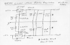
The reg circuit is a result if JBau's experiments and measurements a few years ago on the LT1085, and found that this config handled the stability well without the small tant bypass.
A floating trace is only very loosely coupled to the rest of the circuit so it doesn't matter if it picks up a little RF. It is a good idea to cut just beyond the circuit, provided you won't need to modify the circuit later.
A regulated PSU has lots of amplification so could be upset by RF. Good decoupling is the answer.JonSnell Electronic said:There is no amplification in a power supply so RF is not a problem as there is nothing to upset by way of a tuned circuit/aerial.
I also suggest you change the routing and run at least six vertical strips of "Circuit Common", three on the left and three more on the right, with many horizontal shorting bars all along the length. If you're doing an RF-aware design you definitely want to guarantee that Ground is Ground is Ground is Ground, everywhere...
Since I am running one LT1085 to VDC- by reverse wiring the connection to the other rail, that makes the Reg Output into Common, doesn't it -- so the "low impedance highway to ground" on that rail goes to the Reg Output side.
Or is it late and I'm not thinking clearly? It's slightly counter-intuitive visually.
A floating trace is only very loosely coupled to the rest of the circuit so it doesn't matter if it picks up a little RF. It is a good idea to cut just beyond the circuit, provided you won't need to modify the circuit later.
A regulated PSU has lots of amplification so could be upset by RF. Good decoupling is the answer.
Thanks, good to consider.
Mark said this:
The low level/current input circuits need this to minimise the interference/emi they receive.
The high level/current output circuits need this to minimise the interference/emi they transmit.
This is really important in trying to minimise the loop areas of each circuit.whose length you want to minimize by clever parts placement and routing
The low level/current input circuits need this to minimise the interference/emi they receive.
The high level/current output circuits need this to minimise the interference/emi they transmit.
May I ask what layout tool You are using. The drawing looks very nice and informative.
DIY Layout Creator by bancika. I found it to be straightforward and simple to use but with most of the controls I want. Supports several board types, though does not import from other formats (schematic, excel, etc.) I tried one or two others but struggled with them, when I really just wanted to draw a layout!
Mark said this:This is really important in trying to minimise the loop areas of each circuit.
The low level/current input circuits need this to minimise the interference/emi they receive.
The high level/current output circuits need this to minimise the interference/emi they transmit.
That's a helpful way to think of it.
So I'm trying to get my head around the current flows in the negative rail of this design and how that impacts which leg of that rail needs the lowest impedance path. Not sure if I should post in a separate threadI also suggest you change the routing and run at least six vertical strips of "Circuit Common", three on the left and three more on the right, with many horizontal shorting bars all along the length. If you're doing an RF-aware design you definitely want to guarantee that Ground is Ground is Ground is Ground, everywhere. You want a super low impedance ground network, which also provides a handy place for electric field lines to terminate (a "shield"), so that unwanted coupling is between Node and Ground rather than Node and OtherNode.
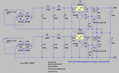
This design is inspired by Wintermute’s config for a dual rail power supply that uses the same positive regular for both rails (YARPS schematic attached). And I’m using LT1085’s with JBau’s circuit for phase, impedance, & symmetry management (also attached).
Normally, each rail would have the current flow through the regulator in certain directions, from In to Out with the Adjust loop performing it's function, and I would make sure of a strong, low impedance path to circuit common (and then shield earth).
But with everything laid out the same for the neg rail and then ONLY reversed at final output, I'm trying to picture it. Now what was Output becomes Common and what was Common becomes Output. The LT1085’s Adjust loop needs a strong reference to Circuit Common to manage the output voltage level well, but it is no longer referencing Circuit Common because the connections are reversed!
Do I still strive for a strong low impedance connection to what would normally be the Circuit Common leg (and ‘Adjust Reference’) leg even though the final output connections reverse the legs of the negative rail?
As you can see I'm getting my head turned around with this.
- Maybe still treat what looks like the 0v leg as common and establish a strong, low impedance path to it. Don’t worry about the fact that the output connection is switched.
- Or maybe treat the regulator leg as the one needing a strong low impedance path, because it is connected to Circuit Common at the Output.
- Or maybe they both need special attention to impedance path.
Wintermute offered: “I think the trick is to forget about the zero volts, It is virtual. just think of current folowing from high to low potential. In the case of the Positive side that will be from the reg through the load and back to the 0v.
“In the case of the neg side it will still be through the reg (which is effectively zero volts) through the load and back via what is the negative rail.”
Reference on basic YARPS design:
You create two identical power supplies. Run them off separate transformer windings and bridge rectifiers, tie what would normally be the ground of the first one to the output of the second one, and what would normally be the ground on the second one becomes your -ve rail. example attached (revised version of my original yarps ps now that I'm a bit wiser... still overkill though).
Attachments
Last edited:
Just a personal remark: I do 100% of my prototypes or one-off's on perfboard, but practically never of the strip variety: stripboards force you into lousy choices and tradeoffs, waste space, and are problematic for the very reasons you invoked, even if in this case they are a minor issue.
I far prefer isolated pads, or even no pads at all: you are free to implement exactly the optimum layout without caring for unforeseen parasitic couplings or bridgetaps.
Even isolated pads become a nuisance when you have to heavily rework a prototype (a kind of truism): they become a mess difficult to shake off from the soldering iron tip.
For sensitive or HF design, the variety having the top layer as a continuous ground plane is ideal.
I think this is the root of your confusion, nothing is being reversed.But with everything laid out the same for the neg rail and then ONLY reversed at final output, I'm trying to picture it. Now what was Output becomes Common and what was Common becomes Output. The LT1085’s Adjust loop needs a strong reference to Circuit Common to manage the output voltage level well, but it is no longer referencing Circuit Common because the connections are reversed!
Yes, but again there is no reversal happeningDo I still strive for a strong low impedance connection to what would normally be the Circuit Common leg (and ‘Adjust Reference’) leg even though the final output connections reverse the legs of the negative rail?
That is because you keep reversing itAs you can see I'm getting my head turned around with this.
Yes, exactlyWintermute offered: “I think the trick is to forget about the zero volts, It is virtual. just think of current folowing from high to low potential. In the case of the Positive side that will be from the reg through the load and back to the 0v.
“In the case of the neg side it will still be through the reg (which is effectively zero volts) through the load and back via what is the negative rail.”
Just a personal remark: I do 100% of my prototypes or one-off's on perfboard, but practically never of the strip variety: stripboards force you into lousy choices and tradeoffs, waste space, and are problematic for the very reasons you invoked, even if in this case they are a minor issue....
Duly noted. My first effort at perfboard was a bit annoying, but I may end up there again... in a future project.
I think this is the root of your confusion, nothing is being reversed.
Perhaps I was not clear. Certainly the Neg rail's regulator-side is connected to Common instead of to Voltage Output as would be normal on a positive rail. So, in that sense, the output connection is reversed in order to achieve a negative rail from a positive regulator.
per Wintermute: “I think the trick is to forget about the zero volts, It is virtual. just think of current folowing from high to low potential. In the case of the Positive side that will be from the reg through the load and back to the 0v.
“In the case of the neg side it will still be through the reg (which is effectively zero volts) through the load and back via what is the negative rail.”
Yes, exactly
This answer helps, and from it I must assume that I should put my particular focus on a low impedance path to the non-regulator side.
Perhaps I was not clear. Certainly the Neg rail's regulator-side is connected to Common instead of to Voltage Output as would be normal on a positive rail. So, in that sense, the output connection is reversed in order to achieve a negative rail from a positive regulator.
Nope. Connect your meter to it exactly the same way as the positive rail and it will read exactly the same. The key words are "potential difference". What do you think is being reversed? Positive, 0V and negative are relative concepts or labels that we have given the difference
Oh, duh... just like any DC battery! Making this way too hard. [emoji51]Nope. Connect your meter to it exactly the same way as the positive rail and it will read exactly the same. The key words are "potential difference". What do you think is being reversed? Positive, 0V and negative are relative concepts or labels that we have given the difference
Sent from my GT-I9505 using Tapatalk
You got it. Any two power supplies can be connected in series like this, negative of one to the positive of the other and we can call the connection 0V. They can be different voltages and different kinds of supplies, even when connected in this way they are essentially separate, with current flowing from positive to 0V and from 0V to negative
Good to see you've got it Bruce "also good to see I wasn't giving you a bum steer!" I struggled with exactly the same thing when I was first "designing" the yarps power supply. I made my layout a mirror image to be symmetrical but I wouldn't advise this now.
AndrewT offered me some advice on the layout (as I also did it on strip board and was unsure what was important) I had all of the -ve side connections just along a strip from load back to the diode bridge. This is not good as there is shared current seen. Ideally the adj cap and 1.12K resistors should connect direct to the load (ie the zero volts point for positive and the -ve output for the negative) and not back along the strip (as is most convenient).
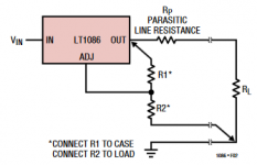
The other one that is important is the connection of the top resistor (100 ohms) you should ideally connect it to the case of the regulator. I soldered mine directly to the out pin of the reg above the circuit board. See below from LT1086 datasheet.
Tony.
I struggled with exactly the same thing when I was first "designing" the yarps power supply. I made my layout a mirror image to be symmetrical but I wouldn't advise this now. AndrewT offered me some advice on the layout (as I also did it on strip board and was unsure what was important) I had all of the -ve side connections just along a strip from load back to the diode bridge. This is not good as there is shared current seen. Ideally the adj cap and 1.12K resistors should connect direct to the load (ie the zero volts point for positive and the -ve output for the negative) and not back along the strip (as is most convenient).
The other one that is important is the connection of the top resistor (100 ohms) you should ideally connect it to the case of the regulator. I soldered mine directly to the out pin of the reg above the circuit board. See below from LT1086 datasheet.
Tony.
Attachments
Last edited:
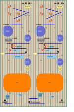
OK so based on the above, This is a rough idea of where I think you should be headed. I'll defer to the more experienced as to whether this is on the right track though! Tripple check that I have made the right connections.. I did it in paint and there is no guarantee I didn't stuff something up (I usually rely on automated check from the schematic to make sure I got everything right!)
Red crosses are cuts to resistor leads, black crosses track cuts. These are just to give the idea of the routing and could be better optimized.
Based on Marks comments on using multiple traces for your zero volts line I think you could optimize the positioning of the links pointed to by the Yellow Arrows.
Tony.
Attachments
- Status
- This old topic is closed. If you want to reopen this topic, contact a moderator using the "Report Post" button.
- Home
- Amplifiers
- Power Supplies
- PSU layout with Vero/Stripboard & RF