I have a few parts on the way for the first prototype, I have ordered a few Welwyn OAR-5 Series Radial Metal Strip Resistor 5mΩ ±1% 5W ±20ppm/°C shunts and a few other misc stuff like smd resistors, 74x CMOS switches signal diodes and adjustable regulators.
http://docs-europe.electrocomponents.com/webdocs/002e/0900766b8002e768.pdf
I have ordered a few general purpose TL072 OP amps for the voltage drive and for the current shunt error amplifiers, I happen to have x2 AD8628 (note I know these are not cheapest they cost $3 each for a dual op-amp), however they have some superior specifications and designed for precision current sensing applications. However looking at the specs the only thing the TL07X is worse is at its Vos (input offset voltage) 10uV VS 15mV
http://www.ti.com/lit/ds/symlink/tl072.pdf
http://www.analog.com/media/en/technical-documentation/data-sheets/AD8628_8629_8630.pdf
Thanks, sure feel free to jump in and join the discussion at any point, I was about to start looking at the SOA figures, you are correct 4 fets for 100Watts is much better than 2.
I'm current looking at these app notes.
http://www.irf.com/technical-info/appnotes/an-1155.pdf
https://www.infineon.com/dgdl/Infineon-ApplicationNote_Linear_Mode_Operation_Safe_Operation_Diagram_MOSFETs-AN-v01_00-EN.pdf?fileId=db3a30433e30e4bf013e3646e9381200
http://docs-europe.electrocomponents.com/webdocs/002e/0900766b8002e768.pdf
I have ordered a few general purpose TL072 OP amps for the voltage drive and for the current shunt error amplifiers, I happen to have x2 AD8628 (note I know these are not cheapest they cost $3 each for a dual op-amp), however they have some superior specifications and designed for precision current sensing applications. However looking at the specs the only thing the TL07X is worse is at its Vos (input offset voltage) 10uV VS 15mV
http://www.ti.com/lit/ds/symlink/tl072.pdf
http://www.analog.com/media/en/technical-documentation/data-sheets/AD8628_8629_8630.pdf
External ADC is all ok. Another version with built in ADC can be discussed later.
Reactance, I can help you with the hardware (mosfets part) if you a bit confused with it. I'm a pro, don't worry.
if you place irfp250n in your list, it is better to use 4 instead of 2 for better breakdown margin.
Thanks, sure feel free to jump in and join the discussion at any point, I was about to start looking at the SOA figures, you are correct 4 fets for 100Watts is much better than 2.
I'm current looking at these app notes.
http://www.irf.com/technical-info/appnotes/an-1155.pdf
https://www.infineon.com/dgdl/Infineon-ApplicationNote_Linear_Mode_Operation_Safe_Operation_Diagram_MOSFETs-AN-v01_00-EN.pdf?fileId=db3a30433e30e4bf013e3646e9381200
Go look at these two devices from Microchip. MCP3551 a 22 bit ADC with preciscion instrument amp built in and could be paired with the PIC18F45K40 (it already has 18 Bit internal ADC if you can live with the poor resolution ")
The PIC also has an internal temperature compensated reference output selectable between 1.024, 2.048 and 4.096V for either internal or external ADC. Read the intro datasheet, it is better that me explaining it. We just completed a similar type of project for accurate temperature measurement.
You can get samples from AVNETKOP. The PIC has built in firmware for comms, PWM etc, with a host of external devices. I used the MCP2221 USB interface. All I/O can be configured analog or digital. Go look at the data sheets it is worth the effort.
These chips and a few external components you can realize the complete project for around US$10 - 15 worth of electronics.
Last edited:
The most critical area is the PCB layout for best screening and best noise performance. You may have to make a few boards to make use of the last few bits of resolution.
For sample chips you can also contact our local Microchip representative Willem Hijbeeck on 011 455 5587 for both samples and support.
For sample chips you can also contact our local Microchip representative Willem Hijbeeck on 011 455 5587 for both samples and support.
In line with Nico Ras I have to say that today I serviced and calibrated some of my multimeters, the cheapest $10 one to 1.5% error in resistor measurement and <0.5% error in the DC 20V and 20mA ranges. With the others error was <0.5% in most cases. In the end lab accuracy is about having voltage references and precision resistors to calibrate equipment which is designed to be calibrated, and after years of use I know exactly how these instruments fail.
Also, I have to say that I have never used ICs from Analog Devices or Linear Tech, most of their products are the kind of chips that someone uses when in an engineering hurry, when unrealistic goals are demanded or when someone wants credit for a product skipping the R&D.
Oh, and a joke: There is even one kind of scientists that pay for having their measuring equipment calibrated, fake scientists.
For now I will use x2 IRFP250 Mosfets, I know this is not recommend and will probably fail in abusive conditions, but as 0.1 prototype lets see how this will play out in the name of education and experience.
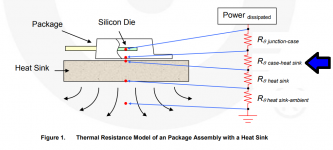
Heat-sink requirements.
===============
The IRF250 has a RθJC (Junction-to-Case ) of 0.7, at 50 watts per device for the two devices.
1) RθJC Junction-to-Case 0.7
175°c - (50W * 0.7RθJC ) = 140.5°c
2) Heatsink RTJA
(140 - 50) / 50W = 1.5°c/W
Note: The heat-sinks will be FAN forced cooled (maybe I will just program the MCU to step the FAN PWM in 3 modes (slow, medium and fast) depending on the programmed temperature for each scale 25°c=25%, 30°c=50%, 50°c=100%)
SOA requirements (per device)
===================
My objective is to keep the temperature at maximum 55°c (RDS will be 1.5Ω approx) for P_max = 50W
P_max = 30Vin_max * I=1.66A
P_max = 1.1Vin_min * I=45A, (use 30A see Shunt Rs_pwr_max)
shunt resistor requirements (P_max = 50W)
============================
Rs_pwr_min = R * I ^ 2 = 0.005 * 1.66^2 = 83mW
Rs_pwr_max = R * I ^ 2 = 0.005 * 30^2 = 4.5Watts
https://www.infineon.com/dgdl/irfp250npbf.pdf?fileId=5546d462533600a4015356288b8b1fde
Last edited:
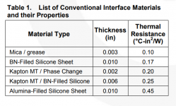
I found these in Fairchild's application note AN-4166, "Heat Sink Mounting Guide"
+
+1 NICE.
It's suicidal to use max Tj for semiconductors, and many commercial designs would not go above 100-120 for Tjmax, but that shouldn't be an issue given you are trying to control heatsink at 50C by fan forcing. Hopefully your heatsink data provides fan-forced design curves, and multiple device derating (if you aren't using separate heatsinks).
A three inch long extrusion of this heatsink (which is 8 inches wide!), has a claimed thermal resistance of 0.66 degC/watt. Add a "skeptical of marketing literature" safety factor and assume it's really 1.0 degC/watt.
If the ambient air is 40 degC, and you're pumping in 50 watts, the heatsink temp will be (40 + (50 \* 1.0)) = 90 degC.
If the mica+grease has a thermal resistance of 0.25 degC/watt for a TO-247 sized piece of mica, and you're pumping 25 watts through each one, then (90 + (25 \* 0.25)) = 96.2 degC at the transistor case.
If each transistor has a junction-to-case thermal resistance of 0.7 degC/watt and you're pumping 25 watts through each one, then (96.2 + (25 \* 0.7)) = 113.7 degC is the junction temperature.
Too high for my comfort! I would get a bigger heatsink, or at least carefully measure this one when pumping in 50 watts and using my exact forced-air configuration. Other designers may feel differently.
Last edited:
A three inch long extrusion of this heatsink (which is 8 inches wide!), has a claimed thermal resistance of 0.66 degC/watt. Add a "skeptical of marketing literature" safety factor and assume it's really 1.0 degC/watt.
If the ambient air is 40 degC, and you're pumping in 50 watts, the heatsink temp will be (40 + (50 \* 1.0)) = 90 degC.
If the mica+grease has a thermal resistance of 0.25 degC/watt for a TO-247 sized piece of mica, and you're pumping 25 watts through each one, then (90 + (25 \* 0.25)) = 96.2 degC at the transistor case.
If each transistor has a junction-to-case thermal resistance of 0.7 degC/watt and you're pumping 25 watts through each one, then (96.2 + (25 \* 0.7)) = 113.7 degC is the junction temperature.
Too high for my comfort! I would get a bigger heatsink, or at least carefully measure this one when pumping in 50 watts and using my exact forced-air configuration. Other designers may feel differently.
Thanks for the comment, you are probably right and I knew this, I was in a hurry and didn't do this first (consult the figures), so now I have a board that can only hold two Fets, the next pcb revision will be based on all the mistakes and leanings from this one, I expect to put X5 IRFP250 per board as I want to make the design modular (its cheaper to manufacturer as well). 100watts per module. and allow them to be stringed. talking about cheap... I might even just drop the external ADC as eva suggested and keep the cost low.
Some heat-sinks show forced cooling vs passive figures, others don't. We pay for the "extra" technical data.
$26,08 Heatsink, 0.4°C/W, 200 x 66 x 40mm, PCB Mount Mount
http://docs-europe.electrocomponents.com/webdocs/14ca/0900766b814ca68a.pdf
vs
$19,43 (I'm going for this heat-sink, its cheap and locally sourced)
PO38555-6063/T6-200 - HEATSINK COMB 34670 NAT 200mm
Last edited:
1) RθJC Junction-to-Case 0.7
175°c - (50W * 0.7RθJC ) = 140.5°c
derating power calculation is missing,
irfp250n PD @25°C is 200W and @50W it will be around 135°C not 175°C
135°C -(50W*0.7°C/W) =100°C
0.7 is typ juction case resistance it can be worse, or even better.
but its all ok, just make it work as v0.1, you can add more mosfet later
Last edited:
There are two kinds of designs: Reference designs and transition designs.
The microchip ADC for measuring instruments just needs an external MUX and costs ~30% of AD chips. I would have performed an extensive search of $ vs. significative bits. I say that because in transition designs there are suboptimal issues for the sake of learning, recycling, shortcutting, or appealing, but if the design has to become a reference later, these suboptimalities would have to be fixed one by one. Optimum learning is obtained by preventing 180deg. turns while evolving a transition design into a reference design. 90deg turns in choices are OK. 360deg turns only happen in case someone deceives the designer.
The microchip ADC for measuring instruments just needs an external MUX and costs ~30% of AD chips. I would have performed an extensive search of $ vs. significative bits. I say that because in transition designs there are suboptimal issues for the sake of learning, recycling, shortcutting, or appealing, but if the design has to become a reference later, these suboptimalities would have to be fixed one by one. Optimum learning is obtained by preventing 180deg. turns while evolving a transition design into a reference design. 90deg turns in choices are OK. 360deg turns only happen in case someone deceives the designer.
the Fairchild heat flow diagram is slightly unusual, in that it shows Rth heatsink thickness.I found these in Fairchild's application note AN-4166, "Heat Sink Mounting Guide"
+
Rth j-c, Rth c-s Rth s-a are all normally shown and using values allows calculation to predict junction and case temperatures.
The extra term Rth htkness shown by Fairchild is normally assumed to be near zero and gets ignored or omitted from the diagram.
For copper and aluminium of normal thicknesses it can safely be ignored.
Where one might add an extra thick spreader plate of use a very thick backplate then follow Fairchild and adopt a value for Rth hthickness and see what comes out.
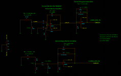
While I wait on the components, I've completed the Current and Voltage front end simulation. This is what I have thus far. I'm busy with the bode plots for the amplifiers, I think I'm on the right track here.
Note: The resistor scaling and PGA might need some reconsideration, as want to minimize errors as much as possible.
Note: The resistor scaling and PGA might need some reconsideration, as want to minimize errors as much as possible.
Attachments
Last edited:
Hi Reactance
I have been watching all of the chatter from the first post. Many good things have come out. I have designed hundreds of Audio Power Amplifiers & Power supplies during my career and the KEY THING WAS $$$. One company I worked for was only concerned with performance and reliability; cost was not the limiting factor.
Don’t cheat on HEATSINK, OUTPUT DEVICES, PROTECTION & DERATING.
Like Mark I purchased a DC LOAD from China and it is a great tool and inexpensive.
You basic schematic shows a SHUTDOWN circuit on the gate and you need a resistor/ferrite to keep it from oscillating.
Keep up the work on the project. Duke
Its still unclear what is shutdown used for. may be it is for quick protection. since turning off mosfet can be done by input.
since protection part is yet designed. will it protect from over volatage, bad connection, pulsed input from continuous tripping PSU test.
I'll try to simulate self protecting mosfet if needed.
since protection part is yet designed. will it protect from over volatage, bad connection, pulsed input from continuous tripping PSU test.
I'll try to simulate self protecting mosfet if needed.
reactance, is your software done?
I can order some MCU and help you designing the mosfets and opamps. Actually 100w doesn't need good heatsink.
Hi ontoaba.
(see attachment)
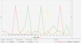
I've put the PC software on hold until the Analog design is actually working 100%. However, see the screen grab, the PC software I gradually started working on a year ago, I was curious at possibly designing an electronic load and played with the concept, now, its a serious project I want to try. The PC client runs on windows only, not sure how much people would want this to run on Linux ? The client is uses the WPF UI stack and looks very appealing to the eye (as it scales on any screen no matter what the screen size is) it also works very well (UI wise).. even better than the commercial BK precision client software which was developed in China which will never receive major software updates doomed by software planned obsolescence.
The MCU firmware I will have to redesign (not a problem for me as I do this stuff for a living, its my daily work domain "windows development and smart phone development"), the original MCU design uses a PIC24FJ128GB210 100PIN device, I don't need a device with this much I/O? (I only used it cause I had this Microchip x2 samples laying around the last 4 years and flirted with the PIC24F stuff) realistically, anything smaller up to ~64-PINS (max) should be used for the following I/O.
ADC_V_MON
ADC_I_MON
ADC_TEMP_MON_1
ADC_TEMP_MON_2
ADC_TEMP_MON_3
ADC_TEMP_MON_4
ADC_VREF_IN
ADC_VREF_TEST
ADC_SELF_TEST
ADC_DAC_TEST
IO_DAC_OUT
IO_FAN_ENABLE
IO_FAN_RPM
UART_DEBUG
UART_COMMS
IO_SPI
IO_I2C
IO_USR_BUTTONS
IO_MISC_FUNCTIONS
IO_MUX_A
IO_MUX_B
Which raises the question what MCU will serve as the replacement part? We are really spoiled for MCU choice, as MCU's for this application requirements are peaking at around ~$6 max mark which is really great, I'm not religious about MCU brands and parts, I will use whatever is suits the requirements, STM32, PIC or MSP430 none of this brands matter to me. (8, 16 or even 32bit) although 16/32-bit is probably better suited for this job as I might end up doing "some" dsp stuff against the ADC's, I don't have personal R&D time to write 8-bit math routines and test them like eva has shown. (it will be great to dedicate time to unlearn what I think I know, and relearn what she has shown that 8-bit mini floats looks interesting)
For this project I'm not keen on assembly though, its just I didn't and don't have the time to learn it so that's only exception.
Again there are so many spanners we can throw this project, but lets focus on the analog design, then map the "Analog board IO" to the MCU.
Attachments
Last edited:
- Status
- This old topic is closed. If you want to reopen this topic, contact a moderator using the "Report Post" button.
- Home
- Amplifiers
- Power Supplies
- DC Electronic Load