Is it the calc sheet that pointed 240mA? Measure your green leds Vf in circuit and if its significantly lower than assumed in the calc it can be due to surely lower current provided to them in circuit by a source resistor degenerated JFET than nominal which is stated for high enough current.
Think of 2-3mA and look up their Vf curve in datasheet to see if its near what you can measure across each. Correct to your original goal with a smaller value CCS set resistor or by paralleling one extra to reach the proper value together. Some spare current is good to have.
I measured 3v79 for the reds D5 & D6 in circuit.
The greens are 5v74 , D2,3,4 .
Get 92mA into load 226r and 150mA across 8r2 (R1).
This looks good to me. Will connect the + reg to the BA-3 preamp and
check it out.
Your mention of a calc sheet got me to thinking, I forgot there was one.
Found it in my saved files and poked in the values...
30Vdc In; 25Vdc out; constant current 150mA; load consumption 116mA;
current source LEDs 5V74; Q3 4.27mA; D1+D5+D6 3V79;R5 1800R
==Gave results of R1=9R1 ; R5(5k pot) 3167R ...
I think I'm good to go!? Will test on preamp in morning.
Thank you for your help.

See the SSLV1.1 guide
http://www.diyaudio.com/forums/power-supplies/192625-sslv1-1-builds-fairy-tales.html
http://www.diyaudio.com/forums/power-supplies/192625-sslv1-1-builds-fairy-tales.html
Hi!
We plan to organize a group buy in Hungary with this version.
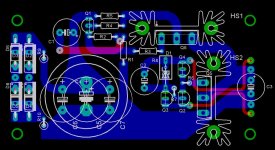
I've designed a PCB as well with the following features:
Regarding parts, values, layout, anything else?
Thanks in advance, cheers!
If it's ready I'am happy to share the eagle files!
Cortez
We plan to organize a group buy in Hungary with this version.
I've designed a PCB as well with the following features:
- on-board AC section (supporting normal and TO-220 cases)
- reference: either with diode (D1) or with trimmer (R8)
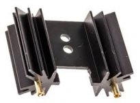
- SK-104 heatsinks
- compact size (doubling it fits the typical 10x10cm PCB size)
- basically single sided design (for DIY etching)
Regarding parts, values, layout, anything else?
Thanks in advance, cheers!
If it's ready I'am happy to share the eagle files!
Cortez
Attachments
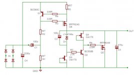
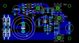
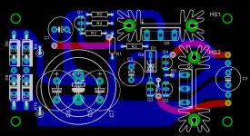
Move R3 to attach to the gate lead.
Turn R6 around to attach closer to the gate lead.
The two links shown in red from Q2/Q3 to the -ve and from Q4/D1 to the +ve should be attached directly to the output nodes over beside C3.
You have high currents passing along the sense leads in your existing proposal. Do not share traces/wires between different circuits.
Nice to have if you can create a bit of space to accommodate
1.) change R5 to two or three resistors in parallel. This allows you to easily change the CCS current and keep the dissipation in the multiple resistors lower.
2.) change the D1 from one Zener to two or three components connected in series. This allows you to fit a LED plus resistor/trimmer plus Zener to set your output voltage.
Thank you Andrew!
BTW: Is there a summary about the different Salas versions?
This is v1.0, there is a v1.1 and maybe a v1.2 in progress..?
For example is there an article about the changes in v1.1?
Regarding theoretical background about the changes and reviews about the SQ as well.
BTW: Is there a summary about the different Salas versions?
This is v1.0, there is a v1.1 and maybe a v1.2 in progress..?
For example is there an article about the changes in v1.1?
Regarding theoretical background about the changes and reviews about the SQ as well.
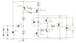
the Salas Shunt regulator is a combination of two circuits.
A Constant Current Source (CCS) that passes the required output current plus some spare current plus the current needed to operate the next stage.
A Shunt regulator stage that is a bit like an adjustable Zener.
If you consider each half alone, you can gain a better understanding of what is needed in each half.
When you come to building, I suggest you build the CCS half alone and leave the whole of the regulator unpopulated. This allows you to set the CCS current and test for correct operation using a shorted output and/or a dummy load. Once you have that working properly and see what minimum voltage drop is required across the CCS, you can populate the regulator half and continue testing.
Yes, much better.
Do you want to keep the separate sense pads? or tie directly into the output pads?
It increases the Builders options, but can lead to errors if they have not read the instructions correctly.
Issue an instruction to insulate the top layer sense tracks to prevent shorting to the heatsink.
Two layers of sticky tape, in addition to the epoxy coating, would be good enough.
Is it okay now? ")
The SK-104 heatsink has an open area right under the transistor section.
The filtering series R after the rectifier diodes (R10) on GND is okay or can cause any problem?
The SK-104 heatsink has an open area right under the transistor section.
The filtering series R after the rectifier diodes (R10) on GND is okay or can cause any problem?
Attachments
Last edited:
"flashes" means what?It is very good indeed, flashes very good in the moment it is turned on.
Is the circuit right or wrong?
Does it blow up?
- Status
- This old topic is closed. If you want to reopen this topic, contact a moderator using the "Report Post" button.
- Home
- Amplifiers
- Power Supplies
- The simplistic Salas low voltage shunt regulator