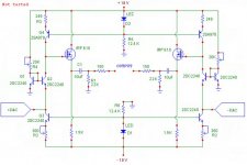
Now that Aleph X projects are well on there way I think a nice dac and passive preamp are all that’s needed to finish the set. When I say dac, all that’s truly needed is the I/V stage as dac schematics are plentiful on the web. My personal favorites are the PCM65, PCM 1702 and for 24bit PCB1704. The I/V for the Aleph X has to be balanced have a low HTD and for my personal tastes have a 2 volt swing for a passive preamp. Here is what I have come up with to get the ball rolling, I’ve taken Jocko Homo’s I/V stage from the Easy-to-build I/V stage thread and made it balanced. The constant current sources share the LEDs or zeners if you like so the noise they make should be the same on both halves. Then, I added the last stage from the Nelson Passes D1 for a nice voltage swing. Following the Nelson Pass philosophy the I/v stage has only 2 semiconductors and one resistor and one cap in the signal path.
I have not built this dac, and it may indeed prove not to work. I am no electrical engineer of I have noooo idea how to even start calculating values for something like this. Because I mostly cut and pasted, most of the values should be right, but I wouldn’t be surprise if the whole thing has to be recalculated and re-biased to make it work. This is just my idea of what the perfect dac to drive an Aleph X amp would look like. It’s my hope that someone will calculate values for this thing and try it or improve on it.
Leve
Attachments
feedback
Hi,
reason for a (very tiny) amount of feedback is that you have to control VERY precicely the I/V factor, especially when going symmetric! both halves of the circuit should be matched far beyond 0.1%, with a feedback of lets say 6dB you are able to match. Otherwise you are a victim to broad tolerances concerning
ß of the first transistor and transconductance of the fet!
IMHO it´s impossible to get symmetric performance without control.
I try to draw and simulate that circuit (UltiCap) and tell you
what happens
") Uli
Uli
Hi,
reason for a (very tiny) amount of feedback is that you have to control VERY precicely the I/V factor, especially when going symmetric! both halves of the circuit should be matched far beyond 0.1%, with a feedback of lets say 6dB you are able to match. Otherwise you are a victim to broad tolerances concerning
ß of the first transistor and transconductance of the fet!
IMHO it´s impossible to get symmetric performance without control.
I try to draw and simulate that circuit (UltiCap) and tell you
what happens
UliUli,
Thank you for your simulation. I see you’ve made some changes. I like the idea of using matched transistors, however there very hard to find. Digi-Key had them; however I don’t think they stock them any more. I will try to find my self an alternative source for these. I don’t really understand what happened to the constant current sources at the top. They seem to have become ways of adjusting the voltage. In Jocko’s “Easy-to-build I/V stage” thread somebody suggested replacing the top constant current sources with a 2.49K resistor and a small cap Jocko said that the distortion would be at least 20 dB higher, I don’t know why, take a look at the thread it’s in the Digital section of this Forum. What happens with the dc offset in reference to ground? That’s still there right?
Let me post a picture of your I/V stage to make it easier for people to see without having to download. I had to make it a little smaller, but you can still see all the values.
Leve
Attachments

Jocko
Jocko announced to be two months off the board, making $$$$$ and was not sure if he would come back.
Hi Thijs,tschrama said:Where is Jocko Homo?!!!!!!!!!
Thijs
Jocko announced to be two months off the board, making $$$$$ and was not sure if he would come back.
voltage source
Leve,
those transistors are voltage sources which define the voltage
on top of the 1k65 resistors, in this case about 20V +-0,2V
which means about 3.5V at the gate -> zero at the source.
Adjust for zero output (DC). you only need to select the led for 1,65V at 2mA. Even tight matching of the fets isn´t necessary,
but select them for about 3,6V G-S at 10mA.If you have Fets with 3,8-4,0V swap 47k with 51k. Intrinsic matching is done by using
MAT´s and 0,1% Emitter resistors.With the 2 1k2 resistors both
halves of the MAT see the same collector-current(->same BE voltage)
Uli
PS: As the DF1704 will be replaced by DF1706 (192kHz 8times
oversampling 24bit) I´m looking forward to make a new DAC
with 4 PCM 1704´s per channel instead of 2, but thats a bit
expensive
Leve,
those transistors are voltage sources which define the voltage
on top of the 1k65 resistors, in this case about 20V +-0,2V
which means about 3.5V at the gate -> zero at the source.
Adjust for zero output (DC). you only need to select the led for 1,65V at 2mA. Even tight matching of the fets isn´t necessary,
but select them for about 3,6V G-S at 10mA.If you have Fets with 3,8-4,0V swap 47k with 51k. Intrinsic matching is done by using
MAT´s and 0,1% Emitter resistors.With the 2 1k2 resistors both
halves of the MAT see the same collector-current(->same BE voltage)
UliPS: As the DF1704 will be replaced by DF1706 (192kHz 8times
oversampling 24bit) I´m looking forward to make a new DAC
with 4 PCM 1704´s per channel instead of 2, but thats a bit
expensive
I don't see why you wouldn't want to simply use the
I/V converter from the D1. Schematics at www.passlabs.com
I/V converter from the D1. Schematics at www.passlabs.com
Nelson Pass said:I don't see why you wouldn't want to simply use the
I/V converter from the D1. Schematics at www.passlabs.com
Because you said that "IT IS NOT INTENDED AS A PROJECT" and we are all very respectful.
Jocko is gone...  so now what I'm gonna do .. I guess this is a bad time to anouce a new, simple, not seen before, (non-original) idea to drastic improve the I/V stage.. I've got a feeling that I've got Jocko's trick now on my computer screen... too bad I can't share it with him... even more bad I can't measure the real performance.. and maybe it is original ... Wel .. if Jocko is alowed to not publish: so am I...
AMT-freak:
Your spot on about the Pass D1 circuit. My ideal I/V stage works of -/+ 5 volt, high PSSR, low THD, low parts-count, no caps.. I/m allmost there.. would you all believe that? Me ? who couldn't even understand the inverting gainclone gain-figure?
I think the D1 I/V stage works very well, but the high Voltage rails make and low PSSR make it more suiteble as an add-on for the BOSOZ...good idea? But I still don't understand why he is addicted to MOSFETs.
AMT-freak: how many I/V-stages have you tried .. I've published 5 or 6 of them .. most of them non-original, but some have a nice feature .. tried any?
As for passive I/V stage: I didn't liked it as much as my simplest active stage? don't now why, may be due to the DAC-chip charateristics..
hmmmmmmm too much beer .. too late... goodnight,
gr,
Thijs
so now what I'm gonna do .. I guess this is a bad time to anouce a new, simple, not seen before, (non-original) idea to drastic improve the I/V stage.. I've got a feeling that I've got Jocko's trick now on my computer screen... too bad I can't share it with him... even more bad I can't measure the real performance.. and maybe it is original ... Wel .. if Jocko is alowed to not publish: so am I...AMT-freak:
Your spot on about the Pass D1 circuit. My ideal I/V stage works of -/+ 5 volt, high PSSR, low THD, low parts-count, no caps.. I/m allmost there.. would you all believe that? Me ? who couldn't even understand the inverting gainclone gain-figure?
I think the D1 I/V stage works very well, but the high Voltage rails make and low PSSR make it more suiteble as an add-on for the BOSOZ...good idea? But I still don't understand why he is addicted to MOSFETs.
AMT-freak: how many I/V-stages have you tried .. I've published 5 or 6 of them .. most of them non-original, but some have a nice feature .. tried any?
As for passive I/V stage: I didn't liked it as much as my simplest active stage? don't now why, may be due to the DAC-chip charateristics..
hmmmmmmm too much beer .. too late... goodnight,
gr,
Thijs
Maybe I was a bit hasty about dismissing this I/V stage. I’m shore Nelson doesn’t care about us building it he just doesn’t want any questions on it e-mailed to him, although he would probably answer them anyway on this site. It certainly looks to be a good design otherwise pass labs would not be selling it and if price is any indicator it was selling for something like $5,000. I didn’t see as many reviews as would I have like to. The reviewer all generally like it, however there was a consensus that the high-end was rolled off. This is most likely because of c40, c33, and c43. I think Nelson put these in there to get rid of HF noise from the dac. I think a diyer may be able to get away without putting these in (feel free to chime in any time here Mr. Pass). Most of this noise is filtered out by the other equipment and the cable in the audio chain, this is 44.1 KHz and 96 KHz noise so to here it you’ll need tweeters that go all the way up.
One fear I do have about using this stage is, the PCM63 outputs 2ma of current, however most other Burr Brown dacs only do 1.2ma. Does some change have to be made to accommodate this, and would this drop the i/v stages voltage swing.
One funny thing about this i/v struck me when I was going threw the Zen balanced line stage article. Mr. Pass notes that distortion is lower with the Zens rails a 60volt’s as compared to 30v. As voltage goes up distortion goes down. So why didn’t he connect R32 to the negative rail that way there will be at least 30v there. Why did he stop at ground?
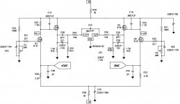
I put this design out there on the “Easy-to-build I/V stage” thread and even redrew it to get all that other stuff out of the way. I only got one reply to it:
I can post this pic as a PDF if anyone wants it .
Leve
One fear I do have about using this stage is, the PCM63 outputs 2ma of current, however most other Burr Brown dacs only do 1.2ma. Does some change have to be made to accommodate this, and would this drop the i/v stages voltage swing.
One funny thing about this i/v struck me when I was going threw the Zen balanced line stage article. Mr. Pass notes that distortion is lower with the Zens rails a 60volt’s as compared to 30v. As voltage goes up distortion goes down. So why didn’t he connect R32 to the negative rail that way there will be at least 30v there. Why did he stop at ground?
I put this design out there on the “Easy-to-build I/V stage” thread and even redrew it to get all that other stuff out of the way. I only got one reply to it:
Ric Schultz said:Yes, I am not only aware of the Pass I-V stage but have tried it. I am concerned by the possiblility of high distortion with the mosfet circuit and also highish noise from the mosfets. That is why I want to try the lower impedance, lower noise and possibly lower distortion bipolar route(soundwise, I really like FETS). The only way to know which circuit sounds best is to try different ones. And tweek them, of course.
So, any suggestions on using the bipolar circuit with a PCM 1738?
Ric Schultz
I can post this pic as a PDF if anyone wants it .
Leve
Attachments
What is interesting about the D1 I/V (besides it being the
only part of the circuit I participated in) is that it simply
cascodes the output of the DAC, the output being a current
source looking for a virtual ground. Thus, it contributes
almost no noise or distortion, and is unbelievably immune
to high frequency (RF) modulation and has no feedback
(just for sex appeal).
Why didn't anybody think of this before? Hell if I know.
It is an obvious thing in retrospect, but nobody seems to
have picked up on it. I blame the educational system for
cranking out "digital only" design engineers.
- Status
- This old topic is closed. If you want to reopen this topic, contact a moderator using the "Report Post" button.
- Home
- Amplifiers
- Pass Labs
- A nice dac to complement the Aleph-X.