PCF has had a definate impact on the way I listen.
I don't think I want to live without that level of driver control.
Of course you can go much farther if you are a FAB*.
I have a nice F7 here with -9 damping factor.
* Fearless Amplifier Builder

This is DIY. 
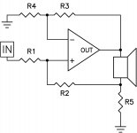
I'll tell what what. Attached is a simple schematic, showing an arbitrarily
simple gain stage.
The damping factor is determined by a confluence of values. LHQUAM
has put together a nice thread discussing this in mathematical detail -
I refer you to his posts.
R3/R4 sets the gain of the "op amp", but it could be a stage with fixed
gain without reference to R3/R4. It could be any sort of non-inverting
power amplifier with reasonable gain, bandwidth and damping factor.
Damping factor is generally influenced by the following:
An increase in the fixed gain of the amplifier will increase the DF
An increase in R1/R2 will increase the DF. Remember that R1 includes
the signal source impedance.
An increase in R5/Rload (speaker) will increase the DF.
As you increase these, the output impedance seen by the load
will down until it literally reaches 0, at which the DF becomes infinity.
More will take you into the region of negative output impedance where
you have negative damping factors, starting with -infinity and proceeding
to "lower" negative DF values.
When you get into the negative region, things get different.
As you go into the negative output impedances the amplifier starts to
exhibit motional control over the voice coil. A DF of -5 has more of this
control than -10, for example.
Low damping factors (like current source amps) encourage acceleration
control. Negative damping factors move you toward velocity control.
So go forth, plug this schematic into your simulators.
Or if you are a paid up member of FAB, wire it up and remember not to
inhale the smoke.
Whoops, I have a reservation at Trink's.
Low damping factors (like current source amps) encourage acceleration
control. Negative damping factors move you toward velocity control.
So go forth, plug this schematic into your simulators.
Or if you are a paid up member of FAB, wire it up and remember not to inhale the smoke.
Interesting Mr Pass and bonne appétit at Trink's !
Do i take risk if huge damping factor velocity force shake drivers too much ? A joke
A reservation at Trinks? This must something new. Maybe you meant St. Orres.
Graeme
Maybe they made an exception. After all, he is the one and only.
")
Odd, that pic was attached at one point or another.
Anyway, here it is.
Trink's. Three nights a week, standing reservation for two.
Here's a painting of our table, courtesy of my sister.
It has a nice view of the ocean.
Anyway, here it is.
Trink's. Three nights a week, standing reservation for two.
Here's a painting of our table, courtesy of my sister.
It has a nice view of the ocean.
Attachments

Do i take risk if huge damping factor velocity force shake drivers too much ? A joke.
Not a joke.
There is a setting beyond which your video is accurate.
There is a setting beyond which your video is accurate.
Like 1812 Overture trick- pause the cd just before the canon shot, turn volume to full on 300w amp, then hit play.
Someone else did the work for me. I just followed along. It looks easy enough to calculate.
Been thinking, will pcf be more of a regular thing now?
I am using positive current feedback [PCF] in a diy Class aP [analog Pulse] amp. The Type 1 scheme posted by lhquam in the thread "First Watt F7 review" was used therein. Will post a blurb in its thread.
The effect of this PCF-enhanced speaker damping on fidelity [clarity, resolution] is truly astounding.
Use PCF in Class D too!
Need to protect the Gate-Source Junction of SJDP120R085
I damaged an SJDP120R085 in a DEF amp during the practice of positive current feedback [PCF] as I had described in earlier posts. The DEF amp was idling at the standard conditions [+/1.3A Id at +/-23Vds] when I made a change [I thought was subtle] which caused it to oscillate driving a loudspeaker.
The original idle Id current [1.3A] dropped to ~50 mA and the output voltage offset rose to >50 mV. The two 2 A fast rail fuses didn't blow.
1. The damaged R085 had developed a substantial gate current.
2. The original value of Vds for each FET was -3.7V [PMOS] and -4.34V [R085]
3. The post damage Vds for PMOS =-3.2V and -3.7V for R085 while using the same resistor string to generate the bias. . This resistor string could no longer sustain the parent Vds values because its flowing current was being drained in a new direction.
4. PMOS was not damaged. A Vds =-3.6 V from a pre-charged 220uF stayed put with time.
5. An initial Vds for R085 = -3.7V from a second pre-charged 220uf began to visibly decrease with time.
A standard 6.2V Zener will protect the Gate -Source junction of R085. It is higher in value than its Pinch-off of -5Vdc. The positive end of the Zener goes to the Source and its negative end goes to the Gate of R085. Recall, that a 100 Ohm resistor is in series with the gate of R085 and will protect the Zener from overcurrent.

The effect of this PCF-enhanced speaker damping on fidelity [clarity, resolution] is truly astounding.
I couldn't agree more. PCF can do real magic for the sound quality.
Cheers,
Johannes
A standard 6.2V Zener will protect the Gate -Source junction of R085.
It is higher in value than its Pinch-off of -5Vdc. The positive end of the
Zener goes to the Source and its negative end goes to the Gate of R085.
Recall, that a 100 Ohm resistor is in series with the gate of R085 and will
protect the Zener from overcurrent.
A zener is standard for the Jfets, even though you are not dealing with the
thin oxide Gate of Mosfets. I have been able to blow out SemiSouth Jfets
and SITs by applying reverse G/S voltage above 40 volts or so.
I lost a couple SIT amps from this early on before I came to realize that there
are actually tube preamps out there that deliver that sort of turn-on/turn-off
transient. A 1 watt 9.1V Zener took care of that, and has been standard for
power Jfets since.
.... A 1 watt 9.1V Zener took care of that, and has been standard for power Jfets since.
Would this also apply to the LU1014s in something like an F3?
Would this also apply to the LU1014s in something like an F3?
Yes, although no F3 has died for lack of it.
- Home
- Amplifiers
- Pass Labs
- DEF Amp