wow, exactly what I was waiting for.Hi all,
After the successful diy assembly of another PASS amplifier (the Aleph 30) and after enjoying it a LOT, I'm very motivated and planning to build the M2.
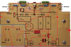
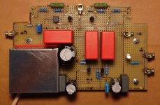
As the M2 has less components I'm thinking on using a 160x100 mm perforated pcb and making point to point soldering with copper wire (it's not the first time I do this, so I feel confident. In fact my TDA1541A nos DAC was made this way).
In any case I would like to share my first sketch of the pcb layout (it's hand-made, sorry for that) just to ensure it's correctness and maybe get some advice.
The overall dimensions of components should be substantially correct. The lines red highlighted with crayon shall be interpreted as galvanic bridges and the view is from above. Two upper corners are to be cut to place the mosfets.
I have a question regarding C2 (10uF). I have at home some MKP big caps and two of them can also be seen in the photo, so I would like to use one of them (the blue or the grey type). The blue is a big 10uF MKP high voltage X2 type and the grey is a Vishay 20uF (700V model 1848). I guess that the MKP shall be the best option in this position (signal path) and I also guess that 20 uF can work as well (or even marginally better regarding the low frequency cut-off) as the 10uF. I'm right?
(I would prefer the 20uF as it's the smaller of the two). View attachment 1241514 .
Many thanks
Thanks for sharing

well, the initial layout changed a bit while building. The final sketch I used to guide myself is attached for convenience.
I added some on-board filtering and later a led (and led series resistor) not indicated in the sketch.
If this can be useful to anybody I'm happy for that, but I haven't tested the board, so cannot say it's 100% right.
If everything is fine red shall be bridges under the board and black shall be the bridges in the upper side. I used 0.8mm copper nude wire (to be tinned before soldering to components), and some thin standard bridges.
Attachments
Hi...help please
M2 Left channel gets between 2 listening session (3 days difference) low?...left channel is very low value..
after check:
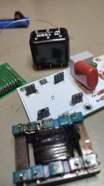
i found out that my auto former PC600/15k is not really working any more. i try to re-solder the thin copper cables (before i put away the isolation) but i had no success. This has 4 windings 2x primary + 2x secondary which are connected like in the original schematic.
as i read here the XS4400 is a very good updated but i cant ordered directly at edcor cost about 42,56USD.
at the European seller (Don-audio) 92 euro excl ship !!!!...holly..**it
so i want to try a cheaper version and found the Hammond 109N (10k with CT :600 with CT). so i have to swap primary and secondary windings. i can leave with factor 1:4 instead of factor 1:5. (600/15k)
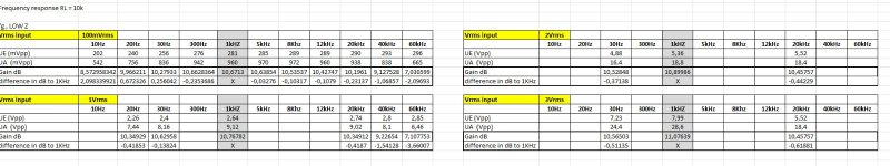
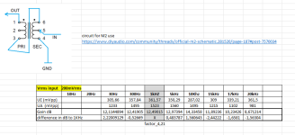
measurements with scope and RL at the 10k load resistor( lower resistors are not working because of bad frequency response):
2Vrms input i got about 18,8Vpp so i got 3,53 factor and about 10.96dB..nearly from 30Hz to 30kHz without drops.....so its fine for me.
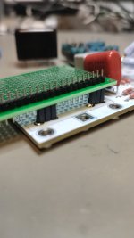
so i think about similar to M2X to build daughter pcb:
i build a kind of daughter board with a small pcb but it doesnt work if i implement this into the place of the original edcor.
How should i implement this into the M2 amp pcb? could i use the CT? it is "just" a CT and not like the edcor PC600/15k 2x prim and 2x sec windings.
i have no clue ...i tried different things but i always got 1:1 ...same signal input as output?
chris
M2 Left channel gets between 2 listening session (3 days difference) low?...left channel is very low value..
after check:
i found out that my auto former PC600/15k is not really working any more. i try to re-solder the thin copper cables (before i put away the isolation) but i had no success. This has 4 windings 2x primary + 2x secondary which are connected like in the original schematic.
as i read here the XS4400 is a very good updated but i cant ordered directly at edcor cost about 42,56USD.
at the European seller (Don-audio) 92 euro excl ship !!!!...holly..**it
so i want to try a cheaper version and found the Hammond 109N (10k with CT :600 with CT). so i have to swap primary and secondary windings. i can leave with factor 1:4 instead of factor 1:5. (600/15k)
measurements with scope and RL at the 10k load resistor( lower resistors are not working because of bad frequency response):
2Vrms input i got about 18,8Vpp so i got 3,53 factor and about 10.96dB..nearly from 30Hz to 30kHz without drops.....so its fine for me.
so i think about similar to M2X to build daughter pcb:
i build a kind of daughter board with a small pcb but it doesnt work if i implement this into the place of the original edcor.
How should i implement this into the M2 amp pcb? could i use the CT? it is "just" a CT and not like the edcor PC600/15k 2x prim and 2x sec windings.
i have no clue ...i tried different things but i always got 1:1 ...same signal input as output?
chris
Attachments
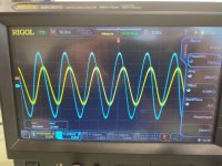
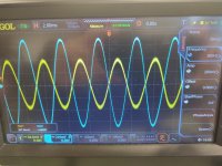
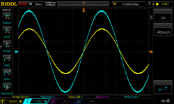
as you can see it is working fine.
test with 100mVrms input and check the input Voltage and output voltage with scope and RL 10K.
at 1Vrms , 2Vrms and 3Vrms i just check the lower and upper frequencies to check the fg response.
test with 100mVrms input and check the input Voltage and output voltage with scope and RL 10K.
at 1Vrms , 2Vrms and 3Vrms i just check the lower and upper frequencies to check the fg response.
Attachments
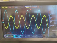
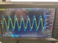
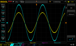
i did the update..
it seems to work_ but over 200mV input i got clipping....hhhmmm...why?
here is the result:
it seems to work_ but over 200mV input i got clipping....hhhmmm...why?
here is the result:
Attachments
-
 109N_fg200mV_1kHz_12,35dB.jpeg248.9 KB · Views: 36
 -
 109N_fg200mV_5kHz_12,97dB.jpeg268.7 KB · Views: 33
 -
 109N_fg200mV_10kHz_14,33dB.jpeg275.8 KB · Views: 31
 -
 109N_fg200mV_15kHz_11,87dB.jpeg285.8 KB · Views: 29
 -
 109N_fg200mV_17kHz_10,32dB.jpeg251.9 KB · Views: 32
 -
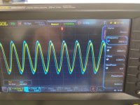 109N_fg200mV_20kHz_8,66dB.jpeg264 KB · Views: 29
 -
 109N_fg200mV_30Hz_12,1dB.jpeg252.1 KB · Views: 30
 -
 109N_fg200mV_300Hz_12,42dB.jpeg274.9 KB · Views: 33
 -
 109N_with CT_for cicuit_M2_measurements.png15.3 KB · Views: 36
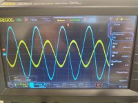
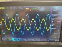
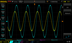
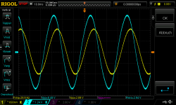
now..here is the test with powered amp:
+/- 22,5V rail, 1,8A bias
10dB
yellow input
blue output inverted
2,8Vrms into 4R gives about 25,5Watt.
because different gm of my Mosfets i got unsymmetrical clipping at max..
PCH is weaker then the N CH...but ...
fg is now 36kHz
old xformer had 55kHz
+/- 22,5V rail, 1,8A bias
10dB
yellow input
blue output inverted
2,8Vrms into 4R gives about 25,5Watt.
because different gm of my Mosfets i got unsymmetrical clipping at max..
PCH is weaker then the N CH...but ...
fg is now 36kHz
old xformer had 55kHz
Attachments
Last edited:
if xformer is connected as autoformer, then there is no phase inversion ( in general, there is some phase change at extremes, but way far from inversion)
same as no phase inversion in input buffer (preceding autoformer) and no phase inversion in output buffer/OS (following autoformer)
it is irrelevant , in this context, that you sort of backward connected xformer, regarding nominal primary and secondary
same as no phase inversion in input buffer (preceding autoformer) and no phase inversion in output buffer/OS (following autoformer)
it is irrelevant , in this context, that you sort of backward connected xformer, regarding nominal primary and secondary
- Home
- Amplifiers
- Pass Labs
- Official M2 schematic