Hi All,
I remember seeing a post by Mr. Pass that the front end JFETs can be replaced by Fairchild J174, J175, P1086 for P channel and Fairchild J111 for N channel. Has anyone tried any of the combinations above, and how's the result?
And if I were to have a go at it (coz I ordered a set of K170 and J74 from china, in case those turned out to be fakes I would have to consider replacements) would I need to make any changes to the circuit to accommodate J174 and J111?
Best regards
Liu
see this : http://www.diyaudio.com/forums/swap-meet/178924-f5-amp-transistor-kit.html
however , regarding your question , look for posts made by jackinnj
however , regarding your question , look for posts made by jackinnj
Thanks Zen Mod. I read through the many posts that a search yielded, and I still havent found the solution I was looking for, mainly because the board that I have now only has space to accommodate 1 device instead of a few paralleled ones (maybe I am not looking at the right posts?). Is there any 1 to 1 substitute that might work? I think I can accept it if the noise performance is not as good as the original part.
BR
Liu
BR
Liu
you can always put 2 parts in space for one , by piggyback approach - one part top of pcb , other at bottom
Idss is what you need to take care of ; say that you need 6-9mA ,while difference in xconductance is what you will have as unavoidable
anyway , in your boots , I would buy originals from h_a or Spencer
Idss is what you need to take care of ; say that you need 6-9mA ,while difference in xconductance is what you will have as unavoidable
anyway , in your boots , I would buy originals from h_a or Spencer
ah.....never thought of that.....
Well, since this is my experimental build, I might just go ahead and put in the set from china. Hopefully I would be able to bias up the amp and hear some music out of it and not blow anything up. Buying originals from one of the 2 gentlemen would probably be the best option when I finished the practice and feel confident enough to start the actual build with diyaudio F5T beta boards which I already have lying there waiting....
Well, since this is my experimental build, I might just go ahead and put in the set from china. Hopefully I would be able to bias up the amp and hear some music out of it and not blow anything up. Buying originals from one of the 2 gentlemen would probably be the best option when I finished the practice and feel confident enough to start the actual build with diyaudio F5T beta boards which I already have lying there waiting....
Yup. I will do that....I assume the method that was discussed in post #11250 of the F5 thread would suffice?
http://www.diyaudio.com/forums/pass-labs/121228-f5-power-amplifier-1125.html#post2796054
http://www.diyaudio.com/forums/pass-labs/121228-f5-power-amplifier-1125.html#post2796054
that will give you Idss.
The bogus jfets test fine for Idss, however the curves do not match between the Pch and Nch devices. This means that the amplifier will run fine, but there will be a difference in distortion between an amp with genuine parts (well matched) and counterfeit parts.
Now, this may not sound all bad. There is a difference between amps built with the Fairchild devices (not exact compliments) and the Toshiba (very close, almost exact compliments). So, I might suggest that there are 4 basic flavors:
- complimentary input + complimentary output
- complimentary input + asymmetrical output
- asymmetrical input + complimentary output
- asymmetrical input + asymmetrical output
Generalizing...
_-_-
Err....this is a bit too deep for me....assuming that the parts that I get are indeed bogus, that would mean that I will have the 3rd flavor, i.e. asymmetrical input + complimentary output (I got the output IRFP240+IRFP9240 from Element14 so I assume that they should be real)? And how bad can the distortion be?
Only the Toshiba output devices show essentially identical transfer curves between N and Pch.
Don't panic.
The distortion will likely be mostly 2nd and 4th harmonic, which sounds good.
I'm not sure if anyone, NP included, has put up distortion spectrum and distortion vs. power for these variations or not. So, I can't give you any figures. But it is clear that the asymmetrical combination in the output stage yields more (mostly even order) distortion. Many people reported preferring the "sound" of the Fairchilds over the Toshiba.
Worst case build with what you have, and change the input devices later. Perhaps consider some high quality sockets for the jfets?? (or some pins in the holes and solder the jfets on top of the board... etc.)
> Only the Toshiba output devices show essentially identical transfer curves between N and Pch.
Not entirely true.
http://www.diyaudio.com/forums/pass-labs/121228-f5-power-amplifier-174.html#post2277700
Patrick
Not entirely true.
http://www.diyaudio.com/forums/pass-labs/121228-f5-power-amplifier-174.html#post2277700
Patrick
Thanks for the insights guys, they give me some comfort that there's still possibility of having a working amplifier (although not optimal performance) with the parts that I got, and the prospects of further experimentation is also very interesting. I think I really need to open up my mind and not be afraid of trying or messing with the board, it's really cool to be able to expect the likely outcome of further experimentation.....
Since you are open to the idea of experimenting with different semiconductors, then I suggest that you solder tack the Through Hole leads to the top of the pads.
Alternatively, insert the very shortest lead through the hole for effective soldering. This will leave LONG leads on the semis when you come to snip them off ready for the next experiment set.
Alternatively, insert the very shortest lead through the hole for effective soldering. This will leave LONG leads on the semis when you come to snip them off ready for the next experiment set.
So, I might suggest that there are 4 basic flavors:
- complimentary input + complimentary output
- complimentary input + asymmetrical output
- asymmetrical input + complimentary output
- asymmetrical input + asymmetrical output
To a large extent P3 will trim any of these to resemble the others.

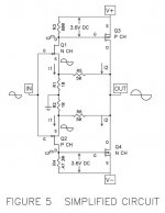
Hi - question for all. What differences need to be made to accommodate a J174/J111 pair in this schematic? Or failing that a piggybacked J174/J111 pair?
The original parts have Idss around 8 ma, and higher transconductance.
You can select these for 10 mA Idss or so, but the open loop gain will be
lower, not that it's a big problem.
Cheers Nelson; much appreciated.
However I have a feeling that the batch of 60 J174/J111's I have are going to be somewhat higher Idss than 10 mA. I haven't sorted them all as yet, but the first few measure a lot higher than that.
So I guess the next question would be what to change in the schematic for a higher Idss part?
However I have a feeling that the batch of 60 J174/J111's I have are going to be somewhat higher Idss than 10 mA. I haven't sorted them all as yet, but the first few measure a lot higher than that.
So I guess the next question would be what to change in the schematic for a higher Idss part?
Attachments
- Status
- This old topic is closed. If you want to reopen this topic, contact a moderator using the "Report Post" button.
- Home
- Amplifiers
- Pass Labs
- F5 Front end JFETs substitute