I found a simplification error in the formula of post 955. Black's formula is correct. The result CLG=5.4 (actually 5.389830508474576) was correct.
"Now lets work out what this implies for the fets transconductance. "
The load resistance is 8 ohms || 60 ohms = 7.0588... ohms. Doing your gm calculation with A=.5*53.3 and Rl=7.0588 Rs=.12 gives gm=6.9S. The R100 Spice model gives gm=7.6S at 1.3A, so we are close. Calculating A from gm=7.6 gives A=28.98, giving an open-loop gain foir both FETs of about 58.
I conclude that all is OK. My measurement of the open-loop gain of 53.3 is probably low due to some other losses in the circuit.
Lhquam, firstly congrats are due for the first build in this thread, your results are inspirational for my efforts. I need a bit of handholding to fill out my understanding so please excuse this rather pedantic post.
...
Again, sorry for the long post...
I'm not convinced there is voltage gain from the top FET? The input is G-S, the output is the Source. It's Common Drain/Source follower
my vote is for
Would that put your calculation results where you think they should be?
")
flg: make believe the upper FET is a SPST switch. A positve voltage = 0.5 V across G-S [Vi] turns it on fully. Current [Io= 1 Ampere] rushes from the positive end of the battery through this FET switch, the load [Rl = 8 Ohms] and finally to ground which is the negative side of the upper rail battery.
- Voltage out = 1 Ampere muliplied by 8 Ohms = 8 Volts
- Av = Vo/Vi = 8 V/0.5 V = 16
- Gm = Io/Vi = 1/0.5 = 2
ZM and others have also explained the above in previous posts. The numerical values that I used are fictional; and real ones are much better.
Last edited:
whatever it is
change upper Jfet with hypothetical P Jfet, so OS is complementary;
is there any difference in functionality ?
I hope that flg is now convinced by your explanation{s] and mine.
Lhquam, firstly congrats are due for the first build in this thread,
OK, I did some more analysis of the open-loop gain calculation. The calculation so far has been a DC analysis. When the transformer inductance and parasitic capacitances, the gate DC blocking capacitors (C5, C6), and operating frequency are taken into account, the open-loop gain is reduced. Not an easy calculation.
That might be good but it's not a SPST switch! The drain of the bottom FET is also part of that upper side load and whatever is at the upper G of that SiCJFET is 1.2V or something lower at the Source. And your telling me it's 8V at the Source with an input of .5V??? The bottom FET better have a gain of 16 or your done!flg: make believe the upper FET is a SPST switch. A positve voltage = 0.5 V across G-S [Vi] turns it on fully. Current [Io= 1 Ampere] rushes from the positive end of the battery through this FET switch, the load [Rl = 8 Ohms] and finally to ground which is the negative side of the upper rail battery.
Whoa! Simultaneous output voltage=8, where did that come from????? the Drain might have 8V because somehow the upper FET has 8Vgs when only fed by.5? But, you might as well put a resistor inplace of the Bottom FET??? If the top FET has 8V on it's Source and the Bottom FET is "OFF", You must have only a 10V rail and your clipping?[/QUOTE]The bottom FET is an open SPST [choked] by comparison [negative turn-off Vi] and/or develops its simultaneous output voltage = 8 which bucks that from the upper FET.
I must be Dumber than ZM but, "Real ones are much better" sounds good to me...ZM and others have also explained the above in previous posts. The numerical values that I used are fictional; and real ones are much better.
I added the input cap to prevent dc across the transformer primary. I changed R5, the resistor to ground, to 100k and it halved lower corner frequency. The 20Hz square wave response is much better with that change.few things:
-toss out that input cap
-put some caps to gnd , after those 1K5 resistors in input buffer's drains
I tried adding the caps across the 1K5 resistors and it made no detectable difference. Since I am testing with switching regulated bench supplies, there isn't much PS noise, but with a "normal" linear PS there will be 120 Hz (and harmonics) ripple. I assume that is why you recommend the caps.
Last edited:
I didn't intend to say "across the 1K5 resistors" . I tested with caps from drains to ground.I meant - put caps from drains to gnd , to make RC of 1K5 and caps ;
without them , you're having swinging drains
flg: kasey197 wrote in post #959 the following
We can see that a 0.5V change in vgs causes Ids to change by 5 to 7 amps depending on vgs. Taking the worst case of 5, this implies transconductance of 5/0.5 = 10S. But the fets transconductance we derived from above observed results (after taking care to correct for source degeneration rs) gives us a measured value of only 4.7 S.
The underlined are real values from the graph kasey197 posted. I used them below to answer your specific question regarding the voltage gain of the upper FET.
- Io= 5 Amperes.
- Vo = 5 Amperes multiplied by Load resistance [ 4 Ohms] = 20 V. I chose 4 Ohms so the calculated Vo is less than a hypothetical positive rail of 25 V [no clipping]. If I chose 8 Ohms instead, then the positive rail voltage is 50 V.
- Av= Vo/Vi = 20/0.5 = 40
I modified from my circuit shown in post 941 as follows: R5 changed to 100K. C5 and C6 have been increased to 62uf (15uf || 47uf). R12 and R15 decreased to 15K. I found that THD decreased by making R12 and R15 smaller.few things:
-toss out that input cap
-put some caps to gnd , after those 1K5 resistors in input buffer's drains
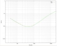
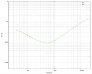
Here are THD vs frequency sweeps with and without the input cap.
The first plot is with input cap, the second without. As you can see, the input cap doesn't seem to degrade things.
Attachments
flg: you wrote above:
Whoa! Simultaneous output voltage=8, where did that come from????? the Drain might have 8V because somehow the upper FET has 8Vgs when only fed by.5? But, you might as well put a resistor inplace of the Bottom FET??? If the top FET has 8V on it's Source and the Bottom FET is "OFF", You must have only a 10V rail and your clipping.
We hopefully agree that both JFETs are matched, and so are the signals to them but; with opposite phase [this debate was over] per Mr. Pass. A positive Vgs happens at the upper JFET, and a simultaneous, and equal negative Vgs happens at the lower JFET. Thus, the channel of the upper JFET opens further and passes additional current through it. By contrast, the channel of the lower JFET closes and removes the same value of pre-existing current flowing through it. The upper JFET has a non-inverting gain of Av [previous post]. The bottom JFET must also have a simultaneous inverting gain of the absolute value of Av. There can only one unique value of output voltage which is Av due to strict matching. The operation of the bottom JFEt is exactly the opposite [closes] as the upper one [opens];clearly noting that the two matched JFETs are operating along a linear Class A trajectory.
If one did not know ahead of time that we're talking about 2 JFETs per the topology of Conceptual F6, one may conclude this [black box] to be one single JFET operating in Class A with a non-inverting gain of Av.
Last edited:
I modified from my circuit shown in post 941 as follows: R5 changed to 100K. C5 and C6 have been increased to 62uf (15uf || 47uf). R12 and R15 decreased to 15K. I found that THD decreased by making R12 and R15 smaller.
Here are THD vs frequency sweeps with and without the input cap.
The first plot is with input cap, the second without. As you can see, the input cap doesn't seem to degrade things.
regarding R12 & R15 - xactly as I told you - you need to find appropriate loading for xformer
regarding input cap - you hear difference ..... or not ; but you'll hardly measure that difference
What he is talking about is a data sheet Vds vs Ids graph. The S is grounded. The gate is fed a constant voltage ref to gnd, and the Vds is sweeped. To save alot of typing, there is no floating Source and Gate Drive like the F6 top FETflg: kasey197 wrote in post #959 the following
We can see that a 0.5V change in vgs causes Ids to change by 5 to 7 amps depending on vgs. Taking the worst case of 5, this implies transconductance of 5/0.5 = 10S. But the fets transconductance we derived from above observed results (after taking care to correct for source degeneration rs) gives us a measured value of only 4.7 S.
Don't worry about me...
regarding R12 & R15 - xactly as I told you - you need to find appropriate loading for xformer
regarding input cap - you hear difference ..... or not ; but you'll hardly measure that difference
Can the transformer be "optimally" loaded by putting the appropriate resistor across the secondary winding and using the high R resistor (R12 and R13) for the bias voltage? That has the advantage of increasing the time constant of R1*C5. I briefly experimented with that, but probably didn't use the right values for loading.
flg: Like you and others, I hope that Mr. Pass explains its operation using verbiage and equations.Disconect the xfrmr from the top FET and tell me what kind of gain you have?
N.B. I failed to mention in my earlier post the following. For the upper JFET, the AC signal from the transformer's secondary rides atop [or floats above] the output signal Vo in real time, and is in phase with it. It is like two AC generators or batteries connected in series. Some may call it bootstrapping? Thus, the upper JFET will always have an AC signal [from the transformer secondary only] between its gate and source and a Vds [positive rail minus Vo+] to operate. In my opinion, the upper JFET uses these two essential variables to deliver a variable output current.
The underlined may further suggest that the bias circuit for the upper JFET needs to be connected to the output rather than to ground; so it also rides up and down on top of Vo like the concurrent AC signal. This bias scheme is clearly shown in OTLAmp1.pdf of post #38. Otherwise, the upper JFET will get cutoff if its bias circuit is referenced to ground!
Last edited:
R1*C5 doesn't have any special relation , at least not for me ;
and that scenario of xformer loading was just one of several , which I already mentioned
which one you'll decide to pursue , is up to you
all will lead to same result - proper loading of secondary , proper gate feed , stable bias
and that scenario of xformer loading was just one of several , which I already mentioned
which one you'll decide to pursue , is up to you
all will lead to same result - proper loading of secondary , proper gate feed , stable bias
upper half bias doesn't need to go to gnd , but output rail
besides that , try to implement "those" few things in second iteration , then hear and measure difference
ZM. I agree. The upper JFET will cuttoff after Vo exceeds the fixed dc value of bias if/when referenced to ground .
- Home
- Amplifiers
- Pass Labs
- F6 Amplifier