Hi,
to avoid capacitors in signal path - that should be possible to use two identical DC current sources.
Drop voltage on each of secondary winding ( Resistance part ) will serve as necessary bias, and final magnetic flux remain 0.
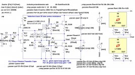
Hopefully Mr.Pass will forgive me that "reuse" of his drawing.
I ran a Spice simulation of your idea and it looks good. The LT3092 regulator looks like it would do the job for the current sources.
Attachments
Yeah, there are probably many other regulators that will work. The LT3092 just happened to be one that I found an application note for and a Spice model.what about tl431. Not as simple but has some history.
buzzforb: I recall TL431 to be a low power regulator. May/will not handle the 43 mA demand multiplied by the rail voltage.what about tl431. Not as simple but has some history.

Dear DIYers. I stand [and sit] corrected about power dissipation. But; TL431 is a shunt regulator; a zener with a dynamic resistance of 0.2 Ohms between its anode and cathode. Thus, it is an AC short between the positive rail and the transformer winding of the upper JFET. The second TL431 is also an AC short between the output and the secondary winding of the lower JFET.
The original suggestor may have envisioned an LM317 positive voltage regulator connected as a constant current source. The Vo output port of LM317 is connected to one end of an 28 Ohm resistor, and the adjustment pin of LM317 is connected to the other end of this resistor. The output current is 1.25 V/28 Ohm = 0.045 A.
The original suggestor may have envisioned an LM317 positive voltage regulator connected as a constant current source. The Vo output port of LM317 is connected to one end of an 28 Ohm resistor, and the adjustment pin of LM317 is connected to the other end of this resistor. The output current is 1.25 V/28 Ohm = 0.045 A.
Last edited:
I found a problem with the LT3092, TL431, and LM134 regulators. The maximum voltage across the devices is 40V, which is not enough for an amplifier with 24 volt rails. Back to the drawing board.
Edit: I might have to backtrack on that observation. Figure 22 in http://www.onsemi.com/pub/Collateral/TL431-D.PDF show the use of an NPN transistor with the TL431 to create a constant current source. The voltage across the TL431 is limited to the voltage across Rcl Plus Vbs of the NPN transistor. The Vce of the NPN transistor must be high enough for rail voltages, in this case, at least 50 volts.
Edit: I might have to backtrack on that observation. Figure 22 in http://www.onsemi.com/pub/Collateral/TL431-D.PDF show the use of an NPN transistor with the TL431 to create a constant current source. The voltage across the TL431 is limited to the voltage across Rcl Plus Vbs of the NPN transistor. The Vce of the NPN transistor must be high enough for rail voltages, in this case, at least 50 volts.
Last edited:
Lhquam. TL783 High Voltage Adjustable Regulator. It has an input - output differential voltage = 125V.I found a problem with the LT3092, TL431, and LM134 regulators. The maximum voltage across the devices is 40V, which is not enough for an amplifier with 24 volt rails. Back to the drawing board.
A series resistor will have a constant voltage across it. When the amplifier output is near the lower rail, the lower current source will stop working. Similarly for the upper rail.it's easy to put resistor in series with CCS , to eat some voltage and keep it safe
not that I'm advocating idea of putting DC through secondaries , even with totaled fluxes
one Jfet will need different bias voltage from another etc.
going simpler isn't simplest always
In my previous post, I should have been more explicit. The upper ccs is where the real problem is. Without using capacitors, I see no way to avoid the upper FET gate approaching the upper rail. There isn't any voltage above to connect the ccs to.nobody tells that you must tie lower CCS to mid-rail/output
you can fed it from upper rail
besides that , if you put cap across that additional resistor .........
anyway - try it , best way to learn .......
@buzz
in BA2 OS , same as in F4 , bias gen is bootstrapped , so it's mid can swing above and below rails
@lhquam - same trick - bootstrap ; somewhere ; maybe across that additional resistor or ....
but - as I'm not for CCS through coil solution , I'll not give you complete schm
in BA2 OS , same as in F4 , bias gen is bootstrapped , so it's mid can swing above and below rails
@lhquam - same trick - bootstrap ; somewhere ; maybe across that additional resistor or ....
but - as I'm not for CCS through coil solution , I'll not give you complete schm
Last edited:
- Home
- Amplifiers
- Pass Labs
- F6 Amplifier