Stupid distortion question. In balanced amp, what causes distortion cancellation? IS it 2K harmonics of equal amplitude, but opposite phase negating each other across the load? Raison I ask, I was wondering if the above were true, you could deliberately mismatch the fets in F1 like circuit and maintain some of the 2K.

Stupid distortion question. In balanced amp, what causes distortion cancellation? IS it 2K harmonics of equal amplitude, but opposite phase negating each other across the load? Raison I ask, I was wondering if the above were true, you could deliberately mismatch the fets in F1 like circuit and maintain some of the 2K.
Would you even need to mismatch the FETs? Or could you just pick well matched fets and mismatch the source resistance (a la F6), and therefore have control over the distortion?
Raison I ask, I was wondering if the above were true, you could deliberately mismatch the fets in F1 like circuit
And (2K-1) ?
(Look, I can handle a lot. But being chased by a tran-something in downtown Frisco at night, and in the meantime he's filling his pants with more family jewelry, that's way over the forrest hill top. I'm just saying.)
Last edited:
And (2K-1) ?
(Look, I can handle a lot. But being chased by a tran-something in downtown Frisco at night, and in the meantime he's filling his pants with more family jewelry, that's way over the forrest hill top. I'm just saying.)
1. Que?
2. What if he has SiT"s in his pants?
1. What happens to uneven harmonics if you misalign rear sight and muzzle.
(lots to learn from watching sea waves, same things that go in amps, SE and balanced stages. with phase-shift added in amps, think a virtual 3d dimension, math becomes the same as nautical stuff)
2. Que ?
(didn't i just say that he suckered me into flying to Cali, and he apparently flew out and SaT on a plane, with dozens of SiT's in his crack)
3. That too.
THnks.1. What happens to uneven harmonics if you misalign rear sight and muzzle.
(lots to learn from watching sea waves, same things that go in amps, SE and balanced stages. with phase-shift added in amps, think a virtual 3d dimension, math becomes the same as nautical stuff)
2. Que ?
(didn't i just say that he suckered me into flying to Cali, and he apparently flew out and SaT on a plane, with dozens of SiT's in his crack)
Maybe it helps not having them, if you know where they have been
 Who knows what those Easter Euro types eat anyway. I have heard they even eat horses.....which, BTW, are in the very famous IKEA meatballs.
1. If sales of Coke goes up, Pepsi goes down
That Easter Euro food is actually pretty good.
(since BA2011, I've had tangible flavor reminiscence visions of the Serbian sausages I had at Vladimir's place. Really WoW)
Back in the day, IKEA shoppers for a large part were the Prius stereotype, made me giggle when I read the thoroughbred-ball news.
(think of me as old-school fckng hippie degenerate, ecological is fine, but never been one for freaky stuff like bio-recycling. So whatever he says, I'm not swallowing any of his SiT crap)
That Easter
Euro food is actually pretty good.(since BA2011, I've had tangible flavor reminiscence visions of the Serbian sausages I had at Vladimir's place. Really WoW)
Back in the day, IKEA shoppers for a large part were the Prius stereotype, made me giggle when I read the thoroughbred-ball news.
(think of me as old-school fckng hippie degenerate, ecological is fine, but never been one for freaky stuff like bio-recycling. So whatever he says, I'm not swallowing any of his SiT crap)
Zen Mod. As always, your brain works great. Your analysis is right on.Can you clean that up a little. It looks interesting, but i dont really know whats going on. Not saying I will when you clean it up, but possibly
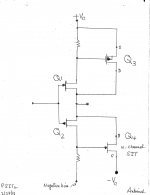
buzzforb. Please find attached [jpg and identical pdf] the cleaned schematic of only the lower option schematic of my previous post. Fortunately, the upper part of the past post schematic was clear, which I hoped maybe useful to Zen Mod or others. Note:
- The circuit is a bare bones schematic which is very much like BA3 Front End and F5/T.
- Unlike BA3 ans F5/T, Q4 in this schematic is a Depletion Mode power JFET; including a SIT. The compound made of Q2 [low power input Depletion PJFET] and the SIT make a quasi power PSIT of unity voltage gain as configured.
- Q1 is a Depletion Mode NJFET which is complementary to Q2. Q1 and the P-Channel power MOSFET Q3 make a compound which may be understood as a power NJFET of unity voltage gain as configured.
- The compound Q1 and Q3 P-MOSFET is where you'll find Schade or Pass negative feedback via the union of the Drain of the P MOSFET and the Source of Q1.
- The SIT may or not need additional Pass feedack. Looks to me that joining the Drain of the SIT to the Source of the input PJFET may also constitute Pass feedback.
- Operate the existing published BA3 FE and F5/T with voltage gain of 1 like the schematic of this post. One thus gets a dual Schade or Pass negative feedback.
- The resulting above 4 possible schematics, PSITa, B3A FE, F5 and F5T are power buffers of adjustable/variable power output. Compare them to the " Beast of a 1000 Jfets" for their simple assembly, relatively obtanium status, and triode-like performance.
Attachments
Your right. I dont know enough to appreciate your designs. I think it would make for a great article. Id give it a go.Zen Mod. As always, your brain works great. Your analysis is right on.
buzzforb. Please find attached [jpg and identical pdf] the cleaned schematic of only the lower option schematic of my previous post. Fortunately, the upper part of the past post schematic was clear, which I hoped maybe useful to Zen Mod or others. Note:
Best regards
- The circuit is a bare bones schematic which is very much like BA3 Front End and F5/T.
- Unlike BA3 ans F5/T, Q4 in this schematic is a Depletion Mode power JFET; including a SIT. The compound made of Q2 [low power input Depletion PJFET] and the SIT make a quasi power PSIT of unity voltage gain as configured.
- Q1 is a Depletion Mode NJFET which is complementary to Q2. Q1 and the P-Channel power MOSFET Q3 make a compound which may be understood as a power NJFET of unity voltage gain as configured.
- The compound Q1 and Q3 P-MOSFET is where you'll find Schade or Pass negative feedback via the union of the Drain of the P MOSFET and the Source of Q1.
- The SIT may or not need additional Pass feedack. Looks to me that joining the Drain of the SIT to the Source of the input PJFET may also constitute Pass feedback.
- Operate the existing published BA3 FE and F5/T with voltage gain of 1 like the schematic of this post. One thus gets a dual Schade or Pass negative feedback.
- The resulting above 4 possible schematics, PSITa, B3A FE, F5 and F5T are power buffers of adjustable/variable power output. Compare them to the " Beast of a 1000 Jfets" for their simple assembly, relatively obtanium status, and triode-like performance.
fat wire from PSU gnd to F6 pcb GND
fat wire from G6 pcb to spk neg. post (NO wire from PSU to neg spk post !)
then bridge made of fat wire between two main GND points of two F6 pcbs
RCA isolated from chassis , coax or twisted pair to pcb
those mains connected NTCs are dangerous - flapping in space and non isolated ; make small pcb for them , place it with screws and extenders on bottom plate
OK...re did the output grounds but I am still not sure by the third statement...between two main GND points of two F6 pcbs...
RCA's are isolated
Rca to PCB is shielded wire.
Still very loud hummmm
Aggravating because my rats nest moskido is dead quiet.
Would adding the buffer help quiet things down?
look where is main gnd point on left channel pcb
now look where is main gnd point on left channel pcb
then connect them with view
after that - use fat wire instead of view
btw. even better if you solder that fat wire

I am not following this. The input G and main GND point (the 4 pads) are all connected in a "T" shape on the bottom side of the board.
OR, are you saying to connect the L and R channel with 1 GND wire and then connect 1 GND wire to Main GND point.
Which then I guess begs the question, should the amp board ground to the PSU PCB ground point or to star ground in chassis?
Still confused...
My wife confirmed they are smart these boards...!
so if there is a lonely housewife in this thread........ buy these boards for your lover!
Generg,
Do you have Jensens as well?
I am not following this. The input G and main GND point (the 4 pads) are all connected in a "T" shape on the bottom side of the board.
OR, are you saying to connect the L and R channel with 1 GND wire and then connect 1 GND wire to Main GND point.
Which then I guess begs the question, should the amp board ground to the PSU PCB ground point or to star ground in chassis?
Still confused...
leave everything as is
connect additional wire from one pcb to another (gnd point on one to gnd point on second)
stop thinking and do what I wrote
think later
Attachments
- Home
- Amplifiers
- Pass Labs
- F6 Amplifier