On BigEs C1x and C2x, 10uf would be very small for suppling current to the output stage. I would just make the wires from the main caps "big and soft metal" (NP) and don't worry about the C1x/C2x caps. Suppling current as close to the draw is good but the capacitance would need to be appropriate to the load.
Steve McCormack uses 1000 uF electrolytics, in the "distributed node archicture" (DNA) series of amps. He "distributes" these 1000 uF caps very close to the output transistors.
I suppose somthing similar can be done here? My worry is creating a power supply that rings.
Are you connecting the V and G of the output boards directly to your PSU or thru the FE boards V and G which is in turn connected to the PSU? I think the answer to C1x and C2x lies therein.
nash
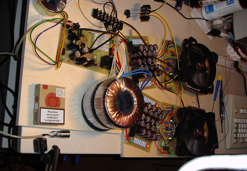
Thanks, I am deciding that at this point. I am thinking to connect the V and G of the output boards directly to the PSU, as the PSU and the FE are on opposite sides of the enclosure. ( This is a 4 pair per channel amp, it is 20" deep ).
The FE boards V and G connect to the output boards, though only one G connection, via either the N or P boards is necessary. The PS is center tapped, and the L/R channel grounds are joined at the center tap.
The speaker hot, would go from the FE board to the speaker protection board, to the binding post.
The speaker return, would go directly from the binding post to the FE board G.
Since the FE board is on the opposite side from the power supply, and all power is being sent down the OP boards power rails, it seems like adding some C1x an C2x to each OP board could be useful.
Looking closer at the boards, it seems that the C1x and C2x would only be necessary if chaining output boards.
You are using two output boards each for N and P respectively arent you?
")
Hi.I am planning to use Elna silmic II 3300uf 50v 30x50mm or Nichicon KG II 10000uF 50v 35x50mm caps for the last C of PS CRC of F5 Turbo V2.Do you think which of them is suitable(or are they suitable for this hot amp because they are rated at 85C) Will they last long?
Or Should i use 105C caps?
I liked elna silmic 2 sound in my 3x paralleled lm3886 amp.Never tried nichicon kg 2.But i am not sure they are suitable for class A amps.Please advise.
Or Should i use 105C caps?
I liked elna silmic 2 sound in my 3x paralleled lm3886 amp.Never tried nichicon kg 2.But i am not sure they are suitable for class A amps.Please advise.
umut,
I've been using the Kendeil's in the full PSU for my F5T V3 that I don't really bother with any other bypass other than what is on the boards.
On my F5 I have the Kendeil's as primary CRC but they have been bypassed with smaller 200uF and 1nF for better transients.
I've been using the Kendeil's in the full PSU for my F5T V3 that I don't really bother with any other bypass other than what is on the boards.
On my F5 I have the Kendeil's as primary CRC but they have been bypassed with smaller 200uF and 1nF for better transients.
I started up the amp tonight. One channel biased up to 150 mV, with .1 mV DC offset. I am sure this can go higher.
The other channel now refuses to do much of anything. The DC offset on the bad channel is stuck around 80 mV, and I cannot get *any* bias current to flow. Both test points measure the same ( slightly below rail voltage ).
on the first attempt, I got the DC offset to go above 3V so the speaker protection kicked in. I can make DC offset go up, but not bias....
The cascode voltage is about the same 14 V, on both sides.
Any ideas on how to proceed with the odd channel behaviour?
I would be most grateful.
Thanks in advance.
I seem to recall that. I bias the channels at 220 mV. However, only one channel has sound.
The silent channel has the same cascode voltages as the running channel, when measuring from the unused jfet pads.
The Gate is connected to the RCA center pin, both measure 1K ohms.
The Source pad of the unused jfet location shows a connection to ground at sensible values: around 10 ohms.
The Drain is connected to the cascode transistor simply because I can measure the voltages. The collector of the N channel cascode transistor is connected to the N-Channel output, so there should be *some* noise coming out.
Does this seem like the jfets are bad to you?
This was the channel that started up oddly.
Can I measure IDSS in circuit?
Last edited:
BigE,
Go through it one stpe at a time, starting at the front. MEasure Idss by checking voltage across 10Rs of the Jfets. It should be in the 6-8ma range. If this is good, make sure you have adjustablilty in the pots, affecting bias adjustment. If this is good, check Vdrop on output Rs. If this is good, then listen. If no sound, then you have a bad connection somewhere. Could not bias output if FE was not generating current
Go through it one stpe at a time, starting at the front. MEasure Idss by checking voltage across 10Rs of the Jfets. It should be in the 6-8ma range. If this is good, make sure you have adjustablilty in the pots, affecting bias adjustment. If this is good, check Vdrop on output Rs. If this is good, then listen. If no sound, then you have a bad connection somewhere. Could not bias output if FE was not generating current
No. It's too complicated to alter the PCB temporarily, to be able to measure Idss...............................Can I measure IDSS in circuit?
This measures Id, not Idss !!!!............ MEasure Idss by checking voltage across 10Rs of the Jfets. It should be in the 6-8ma range. ............
- Home
- Amplifiers
- Pass Labs
- F5 Turbo Builders Thread