The 317 will drop 1.7V by itself. Plus setting resistors. That is its hard limit.
For good specs plus ripple plus some mains tolerance even 5V aren't secure, but if the situation is tight and we just need to shift the DCin a bit it can work, since there will be the CCS next. In general, wrapping a discrete fet & mosfet shunt few elements circuit in an IC defies the concept at least aesthetically. I would just fix the trafo, but if someone does not mind, then can use 317. This is an open project anyway.
For good specs plus ripple plus some mains tolerance even 5V aren't secure, but if the situation is tight and we just need to shift the DCin a bit it can work, since there will be the CCS next. In general, wrapping a discrete fet & mosfet shunt few elements circuit in an IC defies the concept at least aesthetically. I would just fix the trafo, but if someone does not mind, then can use 317. This is an open project anyway.
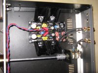
Last night, I parallel mounted a 350R wirewound 25W pot to R1 of the B+.
As soon as I cranked up the current slightly (approx 3ma), the B+ and 5 x LED string went up (jumped approx 0.5V). It looked as if the extra current was shunt by the LED string rather the shunting MOSFET.
I then measured the gate voltage of the shunting FET. It was equal to the B+!!! The 2Sk170BL above the gate was supposed to drop a few volts from the B+, but it didn't. I thought it was toasted. So, I put in an known good one, same result. Then I thought the FET was toasted, put a new one in, still the same.
I checked the jfet and FET that I took out. There was no short. Maybe the FQA12P20's are not suitable, and the quick solution is to use the IR, but I would like to learn something out of this process. Can someone give me some advise what to check next?
Check that there is about 4V Vgs on each gate to source on all Mosfets. This is a pcb, you could not have made wrong connections, they are predetermined. PMOS are at plus side, right? You can not kill a JFET easily there BTW, they are 40V VDS devices. See if the JFET loaded BC550 that drives the gate is OK.
Yup yup, the FQA12P20 are P-channel and are on the plus side (labeled IRFP9240).
Not sure this will help:
1. I have variac in front of the 15-0-15 toroid. I varied the AC input and monitored
the voltages. Measured from "high" pin of R1, both B+ and B- remained very much
constant. B- was at -9.68, and B+ was depending in the R1 value. As long as R1
is not changed, the B+ also stayed at the same voltage. This remained the case
when I changed the AC between 12V and 15V.
2. For the CCS P-MOS Vgs approx 4.7VDC.
For the shunt P-MOS, it is 0, yes, zero, regardless!!!
When I was lowering the R1's resistance, the Vref LED string glowed accordingly
which made me think the current was shunting (or leaking) via the LED string.
The shunt P-MOS is not shunting. The gate is not open??
3. As I cranked up the voltage, the voltage across R1 also went up.
The voltage across B+'s R1 as following
- R1=34R, 0.71V (AC=12V), 0.735 (AC=15V)
- R1 = 29R, 0.658VDC (AC = 12V), 0.672VDC (AC=15V).
Since the CCS's LED string is 5.4, this made me think this FET needs approx
4.7V of Vgs, possible?? What puzzled me is why the jfets on top of the BC550
didn't drop any voltage at all ...
I recommended you see about that 550 first. Change it to be sure. If nothing happens, see about the Jfet under the string of 5. Also that shunt PMOS may be hit. Do you have another? See for any cold soldering and that the pads are OK etc. Is there connection between gate and the rest? Some crack on copper?
debug
also may want to check that R3 is 47R and not 47K...
I recommended you see about that 550 first. Change it to be sure. If nothing happens, see about the Jfet under the string of 5. Also that shunt PMOS may be hit. Do you have another? See for any cold soldering and that the pads are OK etc. Is there connection between gate and the rest? Some crack on copper?
also may want to check that R3 is 47R and not 47K...
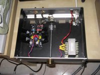
Just completed my second DCB1 with a Wima MKS 1 mF cap.
Transformer this time is an EI core, diodes Schottky, resistors Takkman carbon film, and a DACT 10K attenuator. Also R1 is with one 27 and one 10 ohm resistors.
I can say that this is a big improvement compared to my previous built with normal diodes, LDRs, Takkman carbon film, and a toroid transformer.
Main differences seems to be more extended at the frequency extremes and music seems to be with more body.
Thanks everybody again.
Attachments
I bet they are hot, being smaller than mines and setting more or less the same CCS. Mines are biggers and run quite hot, but you can hold your finger on them without long term burnings 
So WTF!! They are power mosfets, they are made for heavy duty use

BTW, after some weeks of daily usage, all I can say is that the DCB1 is the best preamp I have had in my system. Clear sound, no noise at all and an amazing definition
So WTF!! They are power mosfets, they are made for heavy duty use
BTW, after some weeks of daily usage, all I can say is that the DCB1 is the best preamp I have had in my system. Clear sound, no noise at all and an amazing definition
If it's for the LED, doesn't matter the exact value. Just use ohm law to set it to something between 2 to 15mA, depending of how much light would you like to have.Hey guys,
the 2k2 resistor near the power led is for the led itself right?
I don't have a 2k2 on hand so I'm planning to stick something close in there.
Nice. Are those sinks OK, or too hot? Could go on the box floor too. Especially if reinforced with an aluminum plate. But if its reliable as it is, forget it.
Voltage drop on R1 is 1.9v, so current must be around 260ma. Heat on the fets is 53 celcious max, after been on for 2 days continuously, so I do not worry much. I have my phono shunts run a lot hotter for a bout a year with no problem!
Just an update to my previous saga of attempting to use the Fairchild FQA* counter parts of the IR's. I measured all other transistors and resistors. They all measured correctly, but I replaced them anyway. Unfortunately, the situation did change by much. So, my conclusion is, either I really screwed up something at the board (yeah, I have lifted a few pads out of so many desolderings ) or the P-channel FQA* is not suitable to this use.
I have ordered a few IRFP9240's. Once they arrive, I'll put them in for a quick test. That should tell me one way or the other. If it works, then it will be a forgone conclusion that the Fairchild P-channel is not a direct drop in into this board. Stay tuned!!
) or the P-channel FQA* is not suitable to this use.I have ordered a few IRFP9240's. Once they arrive, I'll put them in for a quick test. That should tell me one way or the other. If it works, then it will be a forgone conclusion that the Fairchild P-channel is not a direct drop in into this board. Stay tuned!!
@vgeorge: mine was dying after some days of usage, some pins almost short when i test using ohmmeter. Better use bigger heatsink IMO.
What temperature did you have on the fets?
I have 2 other shunts and an F5 running hotter than this and survived previous Greek summer with no AC!
- Home
- Amplifiers
- Pass Labs
- Building a symmetrical PSU B1 buffer