your lower mosfet is too much "opened" and output offset is negative because of that
triple-check values of resistors , especially R7
triple check positioning of Jfets
Thanks Zen Mod.
First job this evening will be removing the pcb from the heatsink because it is very difficult to see anything in situ.
I will check the values of resistors. I am pretty sure I checked and measured every resistor before soldering, but will check again! I will also check positioning of Jfets.
Will let you know what I find.
Albert
Haven't you checked for lower mosfets insulation from heatsink?
I have removed pcb from heatsink. Kerafol still stuck to mosfets. Keralfol is larger than mosfet. Hence, no conduction.
your lower mosfet is too much "opened" and output offset is negative because of that
triple-check values of resistors , especially R7
triple check positioning of Jfets
I have removed the pcb from the heatsink and have checked all markings on the resistors. Luckily I used RN55D, so markings are not open to mistakes in identifying colours.
Placement makes it impossible to see markings on R25, R26 and R27 but all others comply with schematic.
Jfets is a bit more difficult. I will upload a photo in a minute and explain.
Albert
Last edited:
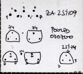
Jfets.
For orientation, I will use R16 to indicate left, R18 for right, IN for bottom and OUT for top.
The jfets are placed using position marked j109.
There are 4 holes from top to bottom on the right.
There are 3 holes from top to bottom on the left.
I used 2 bottom right + bottom left for jfet_1 (flat side towards right).
I used 2 top left and 2nd from top right for jfet_2 (flat side towards left).
The top right hole is unused.
Did I use the right holes?
23:20 Oh, boy. What did I just read about pin 4? I think I have found the error. I should have used all 4 pins on the right and top and bottom on the left (leaving middle unused). Can someone please confirm before I try to desolder the jfets.
If so, does this mean they should both be positioned with flat side to the right?
Attachments
Last edited:
do not turn the fet. bottom one with flat side to the right. top one with the flat side to the left is correct
as far as i know.
Looking at the 2sj109 datasheet, pins 1 and 7 are drain. I think that the way I have mounted them, I used pins 1 and 6!
see
view from top , of course
I used 1, 2, 3 for jfet1
but went wrong when I used 4, 5, 6 (instead of 5, 6, 7) for jfet2!
Time to heat up the soldering iron!
Can I have fried the second jfet or should it be ok?
Lament of a desoldering newbie ...
I have been kicking myself for the last 2 and a half hours but am getting nowhere.
Ah, desoldering
I knew it would not be easy
I have left one jfet in (it was soldered correctly) but tried to get the other one out whole. No such luck.
I ended up cutting/snipping the jfet out (I had left the leads quite long so they should be long enough for re-use) but now have small pieces of the leads in the holes ... and can't get them out
I have used a sharp pin, tried heating with the iron, used wick, ... you get the point. You are probably laughing , because this is such a newb problem.
There is a lot of desoldering info on the web, but nothing I can see that I can use or have not already tried.
I am going to bed
Try again tomorrow. Any suggestions?
Thanks,
Albert
I have been kicking myself for the last 2 and a half hours
but am getting nowhere.Ah, desoldering
I knew it would not be easy
I have left one jfet in (it was soldered correctly) but tried to get the other one out whole. No such luck.
I ended up cutting/snipping the jfet out (I had left the leads quite long so they should be long enough for re-use) but now have small pieces of the leads in the holes ... and can't get them out
I have used a sharp pin, tried heating with the iron, used wick, ... you get the point. You are probably laughing
, because this is such a newb problem. There is a lot of desoldering info on the web, but nothing I can see that I can use or have not already tried.
I am going to bed
Try again tomorrow. Any suggestions?
Thanks,
Albert
Two of the three holes are open far enough that I can see light through them. One is not open enough to mount anything yet. How to open it further?
I tried to push a diode-lead through the hole while heating the other side, but only end up bending the diode leads
The third hole is completely blocked. There is no lead/pin left to grab! What do I do? Buy a very thin drill? Or is there another way?
Sorry for these questions, but I have no idea what to do.
Thanks,
Albert
use a solder sucking pump.
I tried but it did not budge. I think with the 3rd hole a piece of the lead/pin is jammed in the hole.
Left channel working!
Thanks everyone, Zen Mod in particular, for helping me out with this! Much appreciated!
I finally got the third pin out and was able to put the original jfet back in (using the correct holes this time). I now have the left channel back on the heatsink and could not wait to switch it on! I was hoping the rough handling of the pcb and components during my desoldering debacle had not damaged anything and was amazed it is working properly! Incredible how much abuse these things can take!
Rail voltage slowly drifts about 200mV around 27.6V DC and DC offset at speaker output (inputs shorted) is slowly coming down from 56mV to 41mV (after 15-20 mins). Heatsinks quite warm. Will test temperature tomorrow.
Time to go to bed, I think.
Tomorrow or Friday I will take out the right channel and try to do this desoldering stuff a bit better Then I hope to connect the right channel and if everything works out  I hope to have glorious sound.
I cannot wait to compare this new ḧome "built, butchered and built" Aleph J to my original Aleph 3. Will keep you posted.
Thanks again everyone!
Good night
Albert
Thanks everyone, Zen Mod
in particular, for helping me out with this! Much appreciated! I finally got the third pin out and was able to put the original jfet back in (using the correct holes this time). I now have the left channel back on the heatsink and could not wait to switch it on! I was hoping the rough handling of the pcb and components during my desoldering debacle had not damaged anything and was amazed it is working properly! Incredible how much abuse these things can take!
Rail voltage slowly drifts about 200mV around 27.6V DC and DC offset at speaker output (inputs shorted) is slowly coming down from 56mV to 41mV (after 15-20 mins). Heatsinks quite warm. Will test temperature tomorrow.
Time to go to bed, I think.
Tomorrow or Friday I will take out the right channel and try to do this desoldering stuff a bit better
Then I hope to connect the right channel and if everything works out I hope to have glorious sound.I cannot wait to compare this new ḧome "built, butchered and built" Aleph J to my original Aleph 3. Will keep you posted.
Thanks again everyone!
Good night
Albert
Right channel also working
Hi guys,
Wanted to let you know that the second channel is also working. Removing the second jfet was a lot easier than the first and after putting it back into the correct holes, remounting the pcb onto the heatsinks, reconnecting wires (am I glad I used connectors and did not solder the wires to the pcb!) I turned the amp on.
I measure 41.5mV DC at speaker output after 45 mins and with inputs shorted.
Rail voltage has dropped under load from about 30V DC (no load), to 27.6V (left channel only). With both channels it is down to 25.3V. Is it normal that it drops that much?
I have a Fluke 179 and thought I might be able to get some info on the AC ripple by setting the DMM to V AC. I get a reading of about 100mV. Is that OK?
The amp is producing quite a bit of heat! The amp does not yet have feet (the bottom is flush on the desk), so air circulation around the heatsinks is not optimal.
I have checked the temperature and the hottest spot on the heatsinks (after 40 mins; exterior of cabinet) is about 59 Celsius. Ambient is about 26, so about 33 above ambient.
Now I will just let it run in for a while and I hope to be able to listen to it tomorrow or over the weekend.
Not bad for a first ever poweramp build!
Thanks again!
Albert
- Home
- Amplifiers
- Pass Labs
- Aleph J Schematic