You can bypass the whole input section by connecting to IC2B & IC3B (Channel 1 & Channel 2), feedback is also applied at this point.
Hi and thanks and yes this is what i have in mind.
But i do not understand well the connections at the pot.
The signal IN_A goes both to the input of the pot and to the inverting in of the IC2B ... this is strange
Does it mean that i can disconnect the pot and send the signal through C11 directly ?
Anyway i think it could be a wise move after all ... even if i will not be able to use the original inputs.
I haven't analyzed the amp enough to comment on stability if you increase feedback.
My advise is to run a SPICE sim to see what happens
Thanks for the valuable advice. I have already fried a Rotel amp doing this.
I hate these high gains ... it will take me days to put all the schematic in LTSpice but i will try.
Kindest regards, gino
The capacitor forms the input, the 4K7 voltage divider is connected in parrallel with the pot (also a voltage divider). together they control the signal level.
Hi and thanks and it is not an unusual way to connect a volume pot ?
I have always in mind a schema like this one ...
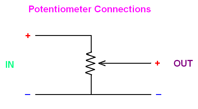
This is much more common wiring scheme i think.
And probably it could have avoided the distortion issue of the video
And i can tell you another thing ... the higher power amps from the same brand use this more usual scheme for the volume control.
Only in for the a500 they have been "naive"
The poor people must suffer ....
Thanks again, gino
Last edited:
I think in the latest revision the 4.7k divider at the input is not there at all.
Can someone trace the whole input topology, including the balanced opamps?
I want to understand what really is going on there, and why it distorts.
Do someone has the full schematic?
Can someone trace the whole input topology, including the balanced opamps?
I want to understand what really is going on there, and why it distorts.
Do someone has the full schematic?
Last edited:
Bump,
Will someone please guide me or send links of how to bias push-pull amps.
There are 3 trim pots on each board, two of them are 2.2k and the other is 100ohm.
Do I need to scope the output and watch for crossover distortion and adjust, or can the process be simpler using just a multimeter?
Thanks.
Will someone please guide me or send links of how to bias push-pull amps.
There are 3 trim pots on each board, two of them are 2.2k and the other is 100ohm.
Do I need to scope the output and watch for crossover distortion and adjust, or can the process be simpler using just a multimeter?
Thanks.
... Do someone has the full schematic?
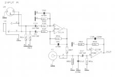
Hi i dont know if it is correct but found this ...
An externally hosted image should be here but it was not working when we last tested it.
Regards, gino
There's a full schematic there, too. Hmm. The basic design strikes me as perfectly sensible - they even thought of providing more supply current for the opamp at high output levels. The balanced input has a pin 1 problem though and as such may appreciate having pin 1 connected to nearest chassis instead.
The opamps on the input board would not seem to be overly stressed. (Impedance imbalance at IC1/4B could be lower, but I wouldn't expect any kind of major distortion from that.) I merely noticed that they skimped on rail decoupling there - scoping the +/-15 V rails at high input levels while varying gain may prove insightful.
The opamps on the input board would not seem to be overly stressed. (Impedance imbalance at IC1/4B could be lower, but I wouldn't expect any kind of major distortion from that.) I merely noticed that they skimped on rail decoupling there - scoping the +/-15 V rails at high input levels while varying gain may prove insightful.
I really want to solve the distortion problem at 50%-80%.
Anyone managed to fix this?
Looking at the full schematic I see the volume pot is sandwiched between two 4580 stages, so it's well buffered and no impedance missmatching can be the cause.
Also, according to google, recent revisions do not have R66 & R67 installed.
Can you please clarify this?
I don't seem to understand what point on the schematic you referring to.
Anyone managed to fix this?
Looking at the full schematic I see the volume pot is sandwiched between two 4580 stages, so it's well buffered and no impedance missmatching can be the cause.
Also, according to google, recent revisions do not have R66 & R67 installed.
I merely noticed that they skimped on rail decoupling there - scoping the +/-15 V rails at high input levels while varying gain may prove insightful.
Can you please clarify this?
I don't seem to understand what point on the schematic you referring to.
Attachments
That's interesting. These would definitely have contributed to input stage (IC1B/IC4B) loading. R66/R67 would be used for pot law bending (read more). Unfortunately it's hard to tell from the naming convention whether they used a lin or log pot, since depending on naming system 20kA could mean either. One would have to simulate things and decide which response would make more sense here, or ask the multimeter.Also, according to google, recent revisions do not have R66 & R67 installed.
Do you see any rail decoupling capacitance around the input opamps (IC1, IC4)? I sure don't, not on the schematic anyway. Not exactly good practice.Can you please clarify this?
I don't seem to understand what point on the schematic you referring to.
In sum, I'd suggest the following:
* Remove R66/67, R71/72
* Add maybe 100 µF, minimum 35 V (better 50 V) from +15V to -15V at both IC1 and IC4, observing polarity
The pot is log.
The decoupling caps between +15v and -15v exist, they called C16 & C30 (100nF) and they are installed in the power supply section.
Any more thoughts about what would make the amp distort and 50-80% on the log pot?
It most certainly in the 4580 preamp sections because when the pot is in the 100& position there is no distortion.
With how much PCB trace in between? Decoupling caps this small are useless when installed at the other end of the known universe, they would have to be right next to each opamp.The decoupling caps between +15v and -15v exist, they called C16 & C30 (100nF) and they are installed in the power supply section.
Actually this much rather points to the power amp input. Input impedance would be minimum at 100%, hence if loading of the previous stages were an issue, distortion would be worst then. Plus, source impedance seen by the amplifier input would be lowest then. Highest source impedance would occur at about -6 dB (about 75% up or so?).Any more thoughts about what would make the amp distort and 50-80% on the log pot?
It most certainly in the 4580 preamp sections because when the pot is in the 100& position there is no distortion.
I just found something that strikes me as somewhat troubling. I hadn't noticed before that this is one of those "upside down" amplifier concepts with floating secondaries. The signal is transferred to the output by way of the output transistors "tugging" on the (floating) +Vcc/-Vcc supplies, whose variation is AC-coupled to the output via the 3300µ/100 caps. There is no DC path to the output.
Now the amplifier does have a DC feedback path. This essentially fixes DC voltage at the +in terminal of IC2B/3B. By contrast, DC resistance seen by the -in terminal varies depending on pot setting, and hence the offset to be expected as a result of input bias current. This is bad because opamp inputs typically need to be kept within about 25 mV of each other in order to avoid unacceptable nonlinearity.
I suppose the 47k resistors R6/7 go some way to addressing this issue under load. Ah, wait, those are the DC path from +/- Vcc back to +in that I was missing earlier.

Hmm, but then it really ought to work. +/-Vcc would just offset a little if need be, and that's that. Except if the voltage at 4580 output were to get so high as to engage the diode limiter, but that shouldn't normally occur.
One would really have to look at what's actually happening around the opamp - signals and supplies. While using a bulb tester in order to keep things from blowing up in case of any mishaps. Plan B, simulate the power amp, where blowing things up is much less of a concern.
") I may actually do that later. I feel we're not that far from a solution to this mystery.
I may actually do that later. I feel we're not that far from a solution to this mystery.Finding problems that the amp designer missed out on can be quite annoying.
Last edited:

It works now.
I deleted one dc supply and instead of ground, -vcc is there.
+vcc and -vcc from a single supply at 75v dc.
As to VR2, I omitted the 50ohm thermistor in parallel with VR2 in purpose.
What you see is the 100 trimpot made from two resistors.
What do you think about the 15v rails, are they inputs or outputs?
The schematic symbols for in or out are the same.
Today in the evening I will draw the full power supply and input opamps, so we will have a fully simulated amp.
I've tweaked this a bit. Needs Mr. Cordell's models (adapt .lib statement if needed). (BTW, VR2 is for bias, while VR1/3 allow tweaking the ratio of T8/9 vs. power transistor bias.)
Actually the circuit works well, even with higher opamp input bias currents, no indications as to why it might misbehave in practice. Nothing, nada, niente, zilch, nichts, rien. I guess that's why it went into production like this.
There is obviously a disagreement between theory and practice here. Routing problems? Layout issues that would have the output strongly couple into the input? (What's transformer wiring look like?) Some part not performing up to spec? I can't imagine that an NJM4580 would have input impedance distortion that severe, it would be much worse than anything Samuel Groner measured.
Looks like there's no way around some measurements after all. Like I said, finding problems that the amp designer didn't can be annoying...
Attachments
You mean T7 T8?BTW, VR2 is for bias, while VR1/3 allow tweaking the ratio of T8/9 vs. power transistor bias.)
I am interested to tweak these in my amp for best performance.
Ratio of what? Power transistor (T9-T12), Not power transistors (T7-T8)...
Can you please elaborate on where and how to measure and adjust these?
*I measure my guitar tube amp (Push-Pull Class AB Marshall) bias current through a 1ohm resistor on the cathodes, but with SS I'm a COMPLETE noob.
In spice, where do I measure the residual current on the push-pull sides?
* From what I can see on the spice model, it is not even a push pull class AB amp, because I don't see a half-sine anywhere.
Thank you.
IMO, the only option left to find the distortion source is to actually run the real amp with a 1k sine and scope it.
Last edited:
I am going to bump this thread one more time with valuable information.
There is a serious problem with the "preamp" stages which generates distortion with the pot is anything but full, and audible noise (elevated noise floor) when the pot is at full but without distortion.
IC1A is the phase canceling stage of the balanced inputs and it also attenuates the signal by 11db (In=1v, Out=0.276v).
IC1B is a boost stage which boost the signal by 8.8db (In=1v, Out=2.76v).
As you can see there is a calculation mistake by Behringer because the two stages should should compensate each other and output the same voltage as the input.
ie: 6db attenuation in IC1A and 6db boost in IC1B.
What they did is to attenuate to 0.276v and boost to 2.76v assuming that the inputs are 1V.
So if we are going to use the RCA jack there will be a boost of the original signal by 8.8db, and if we are going to use RCA plugs through an RCA->TS into the balanced input we will get a 2.2db attenuation of the original signal.
This is only in the two preamp opamps IC1A and IC1B.
After this comes the pot and the Poweramp Opamp IC2B and its feedback loop.
Somehow when the pot is anything but full (some signal goes to ground) there appears a slight harmonic distortion in the signal.
Also, when the pot is at full volume we can hear a hissing sound and various noises from the VU LEDs.
The gain of the power stage by itself is 30db which is very typical for poweramps.
The solution to the distortion and the noise is to simply bypass the preamp stages IC1A, IC1B and the Pot, and simply input right into the poweramp IC2B.
Also disconnect the VU LEDs because they generate interference.
This will utilize the A500 as a straight 30db power amp (like it should be) without it being too loud because of the (mis-calculated) boost stage, and as a bonus the noise floor will remain low.
By the way, many claim ground loop noise when using the RCA jacks.
This amp should be ran with the Ground pin LIFTED to eliminate all hum noise.
If you want to be sure and check against "tingling voltage" you can measure the potential between the ungrounded case and the ground in the wall socket; should be less than a couple of volts.
Our Swedish friends already done this and it works like magic.
faktiskt.se • Visa tråd - Behringer A500 - moddningsoffret
Attached is the final LTSpice version (all included).
Attachments
Last edited:
Uh... What makes you think that?As you can see there is a calculation mistake by Behringer because the two stages should should compensate each other and output the same voltage as the input.
ie: 6db attenuation in IC1A and 6db boost in IC1B.
I am pretty sure that they were shooting for an input sensitivity of +4 dBu (1.23 V) balanced and -10 dBV (300 mV) unbalanced. These are typical nominal "pro" and "consumer" levels. It is not unusual for a studio or PA amp to go down to 0 dBu (0.775 V) balanced even. Yes, that means their total voltage gain is about 6 dB higher than what you'd expect in a consumer amp, but then again consumer amps tend not to have an input level control.
Admittedly it seems a bit dumb to attenuate only to amplify once again, but I've seen much worse. Here in DIN land it used to be common to bring line-level signals down to mic level (with resistors in the 1 Megohm range) in order to feed them through the microphone preamp; this remained common practice in tape gear well into the '80s.
Have you been able to measure anything?
Obviously bypassing the input stage and pot will remove the distortion, but what's causing it in the first place still is totally unclear.
If one intends to keep the balanced input, it would be a good idea to rewire pin 1 from signal ground to chassis ground, if at all possible.
Last edited:
- Status
- This old topic is closed. If you want to reopen this topic, contact a moderator using the "Report Post" button.
- Home
- Live Sound
- Instruments and Amps
- Behringer A500 as a DIY project