A battery header is OK! In fact I sized those 4 holes for a 0.1" header and originally intended to use one, so the battery clips could just be plugged onto the header. That would make the battery wires a bit more break-proof too if the insulation had some support in a header socket. The problem though is all the headers I could find were too tall when the socket was plugged in. I thought about trying a right angle, but it seemd like it would hit the batteries. If you are able to make a header fit, please post some pictures!
Also, something I've been meaning to post in general, might as well twist the two battery clip wires together for each snap. The whole thing is in a metal mint tin so EMI pickup is likely to be nil, but might as well twist the wires anyway.
Thanks. Just wanted to make sure. I have a bunch of generic "Altoids" size tins. I was going to custom etch one for this but I'm on an Art Deco kick right now so I think I'm going to custom build a case from either or a combination of steel, brass and/or zinc. That will allow me to use the headers and JR connector and would end up with a case just a tad larger than the tin.
We'll see once I get the board done.
KD
This may come across ignorant for a first post, and I don't mean it to be so, but I just stumbled across this posting and I've been planning to build a CMOY for a while that is AC powered (simple desktop amp for work) that I''ll eventually add a USB DAC to.
For mine, I intend to power the build using a PCB mount transformer that's 2x12VAC 7VA for the split supply(avel-lindberg ob 14/12). I see the mc78l12acpg in the circuit, and I'm having a bit of trouble wrapping my head around what part I would need to replace it with, if any, assuming modification of the circuit to essentially bypass the voltage drop detection portion.
Thanks in advance!
I was going to custom etch one for this but I'm on an Art Deco kick right now so I think I'm going to custom build a case from either or a combination of steel, brass and/or zinc.
Wow!!
 Please do post some photos when you get it all done!
I see the mc78l12acpg in the circuit, and I'm having a bit of trouble wrapping my head around what part I would need to replace it with, if any, assuming modification of the circuit to essentially bypass the voltage drop detection portion.
Good question! I'll bet there are other folks out there who AC-power their Super CMOYs.
The good news is that all you will have to do is run the +/-DC from your split power supply to the Super CMOY battery connection holes. Everything on the Super CMOY board stays the same. As long was your split supply is more than +/- 7.1Vdc (and less than +/-17Vdc) the low battery protection circuit will think you have fully charged batteries. If you use the alternate set of resistors in the BOM for lithium rechargeable cells it will drop that "low battery" point down to +/-6.26Vdc.
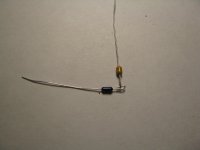
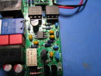
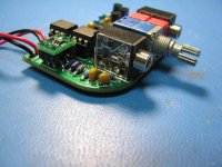
I've attached a picture of the Super CMOY battery wire holes below. What you would do is run the positive DC voltage from your split supply to the bottom terminal of the four, marked "POS", near IC3. Your negative DC voltage from your split supply would go to the "NEG" hole on the other end, near the board edge. Then the common ground wire from your supply would go to either one of the two center battery holes - doesn't matter which one - marked "POS" and "NEG". Be sure to twist all 3 of the wires from your split supply together to help eliminate noise pickup.
And that is it! The OPA1688, the TPS3701, and all the Super CMOY's parts are OK with up to +/-17Vdc power supplies. It would be up to +/-18Vdc, but the MC78L12 is only rated to 35Vdc. For more than the +/-11Vdc you get with two batteries you would have to check on chip power dissipation at very high volume levels with low loads (16R headphones). But for normal listening levels your should be just fine above +/-11Vdc.
The low battery cutoff circuitry is up by those battery input holes. The MC78l12 on the other end of the board is for the headphone relay circuit, which eliminates the turn-on and turn-off pops. Lots going on with that small PC board!
The MC78l12 is there so that the relay's coil always gets a constant 12Vdc regardless of how charged the batteries are - or with an AC supply. A second benefit is providing a constant voltage for the RC time delay parts, so that you get the same 2 second turn-on delay regardless of how charged the batteries are.Attachments
Last edited:
The low battery cutoff circuitry is up by those battery input holes. The MC78l12 on the other end of the board is for the headphone relay circuit, which eliminates the turn-on and turn-off pops. Lots going on with that small PC board!
Thanks for the answer of what that regulator does! I think I'll be able to remove it as I intend to use 12v regulators in the split supply to give me a solid +/- 12vdc..........unless instead the op amp isn't cranky about unregulated ~15.5vdc?
Thanks for the answer of what that regulator does! I think I'll be able to remove it as I intend to use 12v regulators in the split supply to give me a solid +/- 12vdc..........unless instead the op amp isn't cranky about unregulated ~15.5vdc?
Hi, you would still need the MC78L12 because it wires between the rails. So if you have a +/-12Vdc split supply, the MC78L12 gets fed 24Vdc. If you are using your +/-15.5Vdc rails then the MC78L12 gets fed 31Vdc (which is OK). The headphone relay circuit parts and voltages are all relalative to the negative rail, not relative to ground like the rest of the Super CMOY circuitry is. The relay circuit is designed that way so that it doesn't matter if the batteries are fully charged or nearly dead, the relay circuit will work the same way. The MC78L12 only feeds the relay coil and relay control circuit, it doesn't have anything to do with the OPA1688 audio chip's power supply.
You still would need the relay circuit with an AC supply because it is what eliminates the turn-on and turn-off pops in your headphones. As far sas I know there isn't any other CMOY out there with an anti-thump circuit.
Well, as for the unregulated +/-15.5Vdc, give it try!
It would come down to the power supply rejection ratio of the OPA1688, but the PSRR of all modern op amps are typically very good. I wouldn't be surprised if it works just fine. Can't hurt to try it first. If you get hum then add the voltage regulator parts to your power supply.
Last edited:
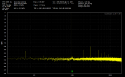
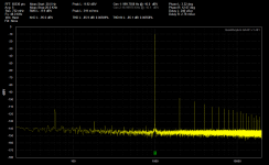
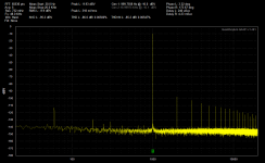
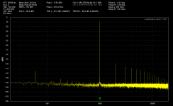
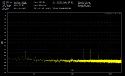
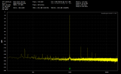
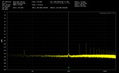
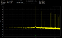
THD+N: primary 9V batteries vs. "9V" lithium polymer - part 1
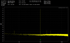
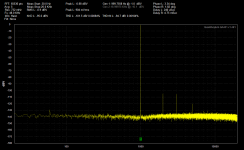
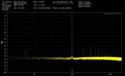
I've been curious what the THD+N for various loads would look like with the Super CMOY running on 9V primary (throw away) batteries vs. the lithium polymer "9V" (7.4 nominal) batteries, given the huge internal resistance difference from the posts above.
The net result: very little difference in THD+N between the two battery types! Likely due to the good PSRR of the OPA1688. But the other take-way here is the OPA1688 is not a happy camper distortion-wise with a 15 ohm load and higher volume levels. Well, it is just a 4mm by 5mm chip after all, with 2 amplifers in it! Pretty impressive overall for such a tiny chip vs. the huge heat-sinked LME49600 buffers on something like the O2 Booster Board or opc's Wire headamp.
Plots:
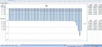
* loopback of the QA401 with -10dBV input and -1dBV input, just to map out the analyzer's own 2nd, 3rd, and at the higher -1dBV input level 5th harmonics. Subtract those from the results. The calculated THD and THD+N is listed at the top of the plot. Remember that you can click ont he arrows in the lower left corner of any of these to zoom it up.
In all of the test results here the 9V primary cells are on the left and the "9V" lithium polymer rechargeable battery is on the right, of each test pair for a given load and input level.
* -10dBV input with a 150R load. Remember from the loopback plots that the QA401's own 2nd and 3rd harmonics at around -122dBV at -10dBV input and around -105dBV at -1dBV input. Pretty large. So with those subtracted out the results due to the Super CMOY here are all under -120dBV. The 4th and 5th harmonics are just a bit less with the lithium polymer batteries.
* -10dBV input with a 33R load. The spray of harmonics from the 3rd on are all under 110dBV. Very similar looking results for the two battery types. Mouse over the plots and you can read the test details in the file name.
* -10dBV input with a 15R load. Everything under about -105eBV. Again very similar looking results for the two battery types.
* -1dBV input with a 150R load. All the harmonics still under -110dBV if you subtract out the analyzer's big 2nd and 3rd harmonics.
I've been curious what the THD+N for various loads would look like with the Super CMOY running on 9V primary (throw away) batteries vs. the lithium polymer "9V" (7.4 nominal) batteries, given the huge internal resistance difference from the posts above.
The net result: very little difference in THD+N between the two battery types! Likely due to the good PSRR of the OPA1688. But the other take-way here is the OPA1688 is not a happy camper distortion-wise with a 15 ohm load and higher volume levels. Well, it is just a 4mm by 5mm chip after all, with 2 amplifers in it!
Pretty impressive overall for such a tiny chip vs. the huge heat-sinked LME49600 buffers on something like the O2 Booster Board or opc's Wire headamp.Plots:
* loopback of the QA401 with -10dBV input and -1dBV input, just to map out the analyzer's own 2nd, 3rd, and at the higher -1dBV input level 5th harmonics. Subtract those from the results. The calculated THD and THD+N is listed at the top of the plot. Remember that you can click ont he arrows in the lower left corner of any of these to zoom it up.
In all of the test results here the 9V primary cells are on the left and the "9V" lithium polymer rechargeable battery is on the right, of each test pair for a given load and input level.
* -10dBV input with a 150R load. Remember from the loopback plots that the QA401's own 2nd and 3rd harmonics at around -122dBV at -10dBV input and around -105dBV at -1dBV input. Pretty large. So with those subtracted out the results due to the Super CMOY here are all under -120dBV. The 4th and 5th harmonics are just a bit less with the lithium polymer batteries.
* -10dBV input with a 33R load. The spray of harmonics from the 3rd on are all under 110dBV. Very similar looking results for the two battery types. Mouse over the plots and you can read the test details in the file name.
* -10dBV input with a 15R load. Everything under about -105eBV. Again very similar looking results for the two battery types.
* -1dBV input with a 150R load. All the harmonics still under -110dBV if you subtract out the analyzer's big 2nd and 3rd harmonics.
Attachments
-
 loopback -10dBV.png43.7 KB · Views: 486
 -
 loopback -1dBV.png43.6 KB · Views: 477
 -
 150R load -1dBV lithium.png44.5 KB · Views: 89
 -
 150R load -1dBV primary.png44.4 KB · Views: 78
 -
 15R load -10dBV lithium.png46.7 KB · Views: 71
 -
 15R load -10dBV primary.png46.9 KB · Views: 81
 -
 33R load -10dBV lithium.png46.1 KB · Views: 75
 -
 33R load -10dBV primary.png46.3 KB · Views: 75
 -
 150R load -10dBV lithium.png45.4 KB · Views: 467
 -
 150R load -10dBV primary.png45.9 KB · Views: 477
Last edited:
THD+N: primary 9V batteries vs. "9V" lithium polymer - part 2
...ran out of photo slots in the post above, part 2.
Same deal as above, the left plot in each pair is the primary 9V batteries, while the right plot is the lithium polymer rechargeable "9V" 7.4 nominal batteries.
* -1dBV input with a 33R load. Not bad at all! 32R is a common headphone / IEM impedance and this is a higher input level.
* -1dBV input with a 15R load. Well... yuk! That is the technical term. Hmmm... worth going back and having a closer look at those OPA1688 THD datasheet curves at 16R load. But at least the chip is still under -105dBV harmonics for lower levels qith a 15R load, above.
I used 33R & 15R rather than 32R and 16R (the datasheet loads) in all these tests just because these are what I had on hand in 1/4W metal film 1%.
The whole purpose of this exercise was to compare the THD+N results of the two battery technologies. From these results is looks like a wash - nearly similar. But the lithium polymer will still provide 3x the capacity. I didn't test any of the NiMH rechargeable cells since their internal battery resistance from the posts above (around 2.2 ohms) wound up between these primary cell (5 ohms) and the lithium (0.4 ohm). I figure that the NiMH results would be inbetween these two.
...ran out of photo slots in the post above, part 2.
Same deal as above, the left plot in each pair is the primary 9V batteries, while the right plot is the lithium polymer rechargeable "9V" 7.4 nominal batteries.
* -1dBV input with a 33R load. Not bad at all!
32R is a common headphone / IEM impedance and this is a higher input level.* -1dBV input with a 15R load. Well... yuk!
That is the technical term. Hmmm... worth going back and having a closer look at those OPA1688 THD datasheet curves at 16R load. But at least the chip is still under -105dBV harmonics for lower levels qith a 15R load, above.I used 33R & 15R rather than 32R and 16R (the datasheet loads) in all these tests just because these are what I had on hand in 1/4W metal film 1%.
The whole purpose of this exercise was to compare the THD+N results of the two battery technologies. From these results is looks like a wash - nearly similar. But the lithium polymer will still provide 3x the capacity. I didn't test any of the NiMH rechargeable cells since their internal battery resistance from the posts above (around 2.2 ohms) wound up between these primary cell (5 ohms) and the lithium (0.4 ohm). I figure that the NiMH results would be inbetween these two.
Attachments

Last edited:
More tips about soldering the TPS3701 boards + Farnell added to BOM + CMOY FR
I have a few more helpful tips for those who want to solder up their own TPS3701 comparator adapter boards.
I tried a finer tip on the soldering station weeks ago and found it didn't really help, the tiny leads on the TPS3701 still flooded and needed solder wick after to clean up. Then I remembered a few days ago that finer gauge solder exists. I use a 0.022" (=0.56mm) eutectic silver-bearing solder for most things (63/36/2). The next standard size down is 0.015" (=0.38mm). I had also forgotten that I had a bunch of it, I just never use it because - until now - it is too thin, requiring several inches to be fed to a normal sized joint.
Well it turns out 0.015" solder is just the ticket for the SOT-23-6 package. Now with a finer tip (1/64" = 0.4mm conical) I can individually solder nearly every pin on the chip. I'm down to solder briding maybe 2 pins on each chip rather than all pins on both sides. All of this is done under a magnifying glass too.
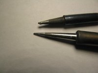
The first photo shows the 1/32" (= 0.80mm) conical tip and the original 0.022" solder. The bottom half of the photo shows the new 1/64" conical tip and the 0.015" solder
The next two photos are close-ups of the solder and soldering station tips. The 1/64" doesn't hold much heat, but not a lot is needed either for the tiny chip and thin solder.
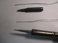
The next photo shows a handy type of tweezer. The black sharp ones at the top are the tweezers I use for most things. The stainless pair with the flat tips are a Hakko 107-SA from Amazon.com for around $17. The tips are specifically designed to pick up small SMD parts. If anyone knows of other tweezers out there designed for SMD, please post! The tweezers at the top work great for standard SOIC8 (like the OPA1688), but are completely useless for the tiny SOT-23-6. The chip just flies off the end in all directions.
In some other Super CMOY project news I have yet another revised BOM posted at the Google Drive link in the first post in this thread. On this BOM update I've added a Farnell column and started filling it in, which may help folks outside of the US.
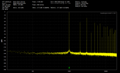
And finally in the THD tests above with the two types of batteries I also ran a frequency response test on the CMOY using the QA401. Results below. Flat as a board up to 22KHz. The test was from 10Hz to 25KHz in 500Hz steps using the QA401.
I have a few more helpful tips for those who want to solder up their own TPS3701 comparator adapter boards.
I tried a finer tip on the soldering station weeks ago and found it didn't really help, the tiny leads on the TPS3701 still flooded and needed solder wick after to clean up. Then I remembered a few days ago that finer gauge solder exists. I use a 0.022" (=0.56mm) eutectic silver-bearing solder for most things (63/36/2). The next standard size down is 0.015" (=0.38mm). I had also forgotten that I had a bunch of it, I just never use it because - until now - it is too thin, requiring several inches to be fed to a normal sized joint.
Well it turns out 0.015" solder is just the ticket for the SOT-23-6 package. Now with a finer tip (1/64" = 0.4mm conical) I can individually solder nearly every pin on the chip. I'm down to solder briding maybe 2 pins on each chip rather than all pins on both sides.
All of this is done under a magnifying glass too.The first photo shows the 1/32" (= 0.80mm) conical tip and the original 0.022" solder. The bottom half of the photo shows the new 1/64" conical tip and the 0.015" solder
The next two photos are close-ups of the solder and soldering station tips. The 1/64" doesn't hold much heat, but not a lot is needed either for the tiny chip and thin solder.
The next photo shows a handy type of tweezer. The black sharp ones at the top are the tweezers I use for most things. The stainless pair with the flat tips are a Hakko 107-SA from Amazon.com for around $17. The tips are specifically designed to pick up small SMD parts. If anyone knows of other tweezers out there designed for SMD, please post! The tweezers at the top work great for standard SOIC8 (like the OPA1688), but are completely useless for the tiny SOT-23-6. The chip just flies off the end in all directions.
In some other Super CMOY project news I have yet another revised BOM posted at the Google Drive link in the first post in this thread. On this BOM update I've added a Farnell column and started filling it in, which may help folks outside of the US.
And finally in the THD tests above with the two types of batteries I also ran a frequency response test on the CMOY using the QA401. Results below. Flat as a board up to 22KHz. The test was from 10Hz to 25KHz in 500Hz steps using the QA401.
Attachments
Last edited:
1x gain rework instructions forV4.0 boards
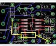
If you have one of the existing V4.0 Super CMOY boards and want to set it for 1x gain, here is some re-work instructions on how to add the 1nF capacitor that johnc124 calculated in a post above. Note that this is ONLY for 1x voltage gain (run as just a current buffer). If you are using any other gain, like 1.5x, 2x, 3x, 4x, etc. you don't need this. The board is fine the way it sits. This addition just increases the phase margin a bit in the specific case of 1x voltage gain. The new V4.1 boards have a place for this capacitor already on the board, but again it is only needed if you set the headamp for 1x gain.
The first photo shows the parts involved. The existing 825R resistor in for R8 and R9 on the top of the photo, plus the new 1nF (= 1000pF = 0.001uF) axial, 50V, 5% C0G MLCC cap, Mouser #581-SA105A102JAR for $0.33 each. The capacitor is about the same physical size as the 1/8W resistor.
What you will be doing is unsoldering one end of R8 and R9, pulling it out of the Super CMOY PC board, then soldering that end onto one end of the 1nF capacitor. The 2nd and 3rd photos shows a good way to do that. I typicall bend small hooks in each lead, the hook them together and cut off the excess before soldering them. For R9 the two should be soldered at a right angle like picture #2. For R8 bend the capacitor back on top of the resistor before soldering them together.
The first plot shows what to do with R9. Unsolder that top lead with the yellow circle around it by using the soldering iron tip to heat the lead why prying it up and out of the PC board. Then solder it to one end of the capacitor (that yellow rectangle in the plot) and finally the other end of the cap to the left end of R6, which is the chip non-inverting input. Just solder it right on to existing R6 lead, no need to remove that one.
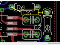
R8 is similar. Unsolder the right end, solder it to a 1nF capacitor which sits on top of R8, then attach the free end of the capacitor to the bottom end shown of R7, which is the other OPA1688 non-inverting input. For that long wire run from the cap to C7 you may want to insulate it with heat shrink tubing, or just a length of insulation stripped off another wire and slid back over the capacitor lead.
If you have one of the existing V4.0 Super CMOY boards and want to set it for 1x gain, here is some re-work instructions on how to add the 1nF capacitor that johnc124 calculated in a post above. Note that this is ONLY for 1x voltage gain (run as just a current buffer). If you are using any other gain, like 1.5x, 2x, 3x, 4x, etc. you don't need this. The board is fine the way it sits. This addition just increases the phase margin a bit in the specific case of 1x voltage gain. The new V4.1 boards have a place for this capacitor already on the board, but again it is only needed if you set the headamp for 1x gain.
The first photo shows the parts involved. The existing 825R resistor in for R8 and R9 on the top of the photo, plus the new 1nF (= 1000pF = 0.001uF) axial, 50V, 5% C0G MLCC cap, Mouser #581-SA105A102JAR for $0.33 each. The capacitor is about the same physical size as the 1/8W resistor.
What you will be doing is unsoldering one end of R8 and R9, pulling it out of the Super CMOY PC board, then soldering that end onto one end of the 1nF capacitor. The 2nd and 3rd photos shows a good way to do that. I typicall bend small hooks in each lead, the hook them together and cut off the excess before soldering them. For R9 the two should be soldered at a right angle like picture #2. For R8 bend the capacitor back on top of the resistor before soldering them together.
The first plot shows what to do with R9. Unsolder that top lead with the yellow circle around it by using the soldering iron tip to heat the lead why prying it up and out of the PC board. Then solder it to one end of the capacitor (that yellow rectangle in the plot) and finally the other end of the cap to the left end of R6, which is the chip non-inverting input. Just solder it right on to existing R6 lead, no need to remove that one.
R8 is similar. Unsolder the right end, solder it to a 1nF capacitor which sits on top of R8, then attach the free end of the capacitor to the bottom end shown of R7, which is the other OPA1688 non-inverting input. For that long wire run from the cap to C7 you may want to insulate it with heat shrink tubing, or just a length of insulation stripped off another wire and slid back over the capacitor lead.
Attachments
Last edited:
Adafruit knobs & case + V4.1 boards + my mistake on the 15R THD & -1dBV input
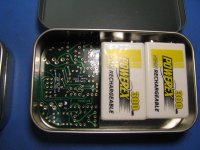
Adafruit knobs and mint tin
The slim knobs arrived from Adafruit and they work perfectly! I also ordered some of their "blank" mint tins to try out. Their mint tins really are the same size as the standard mint tin. Something to keep in mind for folks wanting to do their own artwork on the tin!
The first 3 photos show the new knobs, 10mm long and 15mm long, #2058 and #2057 at adafruit.com for $0.95. You can just enter those numbers right into their search box and it will come up with the parts. The diameter of the knobs is just slightly less than the width of the volume pot, which is perfect.
The next two show their blank mint tin, #97 for $2.50. Fits great!
I have some of the knobs and mint tins now I'll be adding to the sales list at my vendor thread, just at-cost.
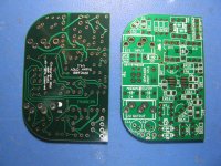
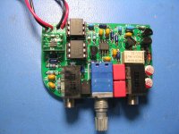
V4.1 PC boards back from fabrication
In other project news the V4.1 PC boards are back, below! I'll build one up over the weekend and make sure there are no layout errors. I'm in the process of modifying the BOM, build instructions, and other materials out at the Google Drive link to be combined V4.0 and V4.1. The only significant difference between the two board versions are the C13 and C14 capacitors that implement johnc124's fix for 1x gain, if someone wants to use 1x gain. The rest of the changes are just minor cosmetic stuff with the silk screen part markings. If you have a V4.0 board and want 1x gain, just follow the re-work intructions in a post above to easily add those two capacitors.
Discussion of the 15R load THD results and mistake in the -1dBV level
And finally I've figured out what went wrong with the 15R load THD measurements in post #88 above. Operator error!
First off, on the 33R and 150R load tests at -1dBV measurements I actually had the amplifer adjusted to +1dBV rather than -1dBFS, which means 1.1Vrms rather than 0.9Vrms. That shows up if you zoom in on any of those -1dBFS measurements and go up to the text at the top in the middle. The 15R load was currectly at -1dBV though.
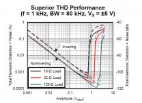
The big problem with the 15 ohm tests is that I simply had the input level up above what the OPA1688 chip is rated for. At the 0.9Vrms input that would be 1.27V peak output. Into a 15R load that gives 1.27V/15R = 85mA, 10mA more than the maximum rated 75mA output of the OPA1688, resulting in the high level of harmonics. So the chip was doing exactly what it is supposed to do, the input level just went above max ratings. I should have limited the input in the 15R load case to 0.8Vrms = 800mVrms, 0.1mV less that what I was using, to stay under 75mA output.
From the datasheet THD curves below the "knee" of the 16R THD curve (black line), where it hits the output current maximum and shoots up, is around 0.65Vrms. But that is with +/-5Vdc power rails. The Super CMOY was running with around +/-8Vrms on the lithium polymer batteries, which will shift the maximum level of the knee up a bit to the 0.8Vrms.
The THD measurements at the 3 different loads matched up well with this datasheet curve. The curves show the 16R with higher distortion than the 32R, and that higher than the 128R. The actual results were similar for 15R, 33R, and 150R.
Adafruit knobs and mint tin
The slim knobs arrived from Adafruit and they work perfectly! I also ordered some of their "blank" mint tins to try out. Their mint tins really are the same size as the standard mint tin. Something to keep in mind for folks wanting to do their own artwork on the tin!
The first 3 photos show the new knobs, 10mm long and 15mm long, #2058 and #2057 at adafruit.com for $0.95. You can just enter those numbers right into their search box and it will come up with the parts. The diameter of the knobs is just slightly less than the width of the volume pot, which is perfect.
The next two show their blank mint tin, #97 for $2.50. Fits great!
I have some of the knobs and mint tins now I'll be adding to the sales list at my vendor thread, just at-cost.
V4.1 PC boards back from fabrication
In other project news the V4.1 PC boards are back, below! I'll build one up over the weekend and make sure there are no layout errors. I'm in the process of modifying the BOM, build instructions, and other materials out at the Google Drive link to be combined V4.0 and V4.1. The only significant difference between the two board versions are the C13 and C14 capacitors that implement johnc124's fix for 1x gain, if someone wants to use 1x gain. The rest of the changes are just minor cosmetic stuff with the silk screen part markings. If you have a V4.0 board and want 1x gain, just follow the re-work intructions in a post above to easily add those two capacitors.
Discussion of the 15R load THD results and mistake in the -1dBV level
And finally I've figured out what went wrong with the 15R load THD measurements in post #88 above. Operator error!
First off, on the 33R and 150R load tests at -1dBV measurements I actually had the amplifer adjusted to +1dBV rather than -1dBFS, which means 1.1Vrms rather than 0.9Vrms. That shows up if you zoom in on any of those -1dBFS measurements and go up to the text at the top in the middle. The 15R load was currectly at -1dBV though.
The big problem with the 15 ohm tests is that I simply had the input level up above what the OPA1688 chip is rated for. At the 0.9Vrms input that would be 1.27V peak output. Into a 15R load that gives 1.27V/15R = 85mA, 10mA more than the maximum rated 75mA output of the OPA1688, resulting in the high level of harmonics. So the chip was doing exactly what it is supposed to do, the input level just went above max ratings. I should have limited the input in the 15R load case to 0.8Vrms = 800mVrms, 0.1mV less that what I was using, to stay under 75mA output.
From the datasheet THD curves below the "knee" of the 16R THD curve (black line), where it hits the output current maximum and shoots up, is around 0.65Vrms. But that is with +/-5Vdc power rails. The Super CMOY was running with around +/-8Vrms on the lithium polymer batteries, which will shift the maximum level of the knee up a bit to the 0.8Vrms.
The THD measurements at the 3 different loads matched up well with this datasheet curve. The curves show the 16R with higher distortion than the 32R, and that higher than the 128R. The actual results were similar for 15R, 33R, and 150R.
Attachments
Last edited:
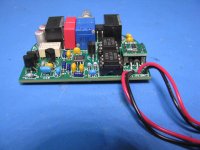
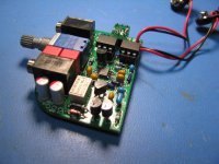
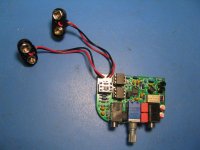
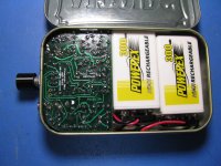
V4.1 works! Revised BOM and Build Instructions available
I've built up and tested a V4.1 board now. Works perfectly! I built it up with 1x voltage gain too (current buffer) using johnc124's 1nF compensation caps back to the input.
I've used the solid molded Keystone 235-M battery snaps on this one. I really like these snaps. So much easier to get on and off the batteries. I have them listed in the BOM now.
Which reminds me.. I've continued to update both the BOM and Build Instructions out at the project Google Drive link in the first post in this thread. I did a significant update to the build instructions over the weekend, lots more information in there now. I have the details included now for using - or not using if you want more than 1x gain - the 1nF compensation capacitor. I've added a section on "options" to decide on before the build, such as which battery type you plan to use (which determines the resistor set for the comparator in the BOM), which voltage gain level (determines the gain resistor set in the BOM), and the LED options.
I've added a couple of things to the BOM yesterday and today. The 2N7000 mosfets and the 12V regulator in the headphone relay circuit section are now specified with part numbers that have pre-formed leads to fit perfectly in the board holes without any bending. That just leaves the depletion mosfet in the current source as the remaining TO-92 the leads need to be bent slightly. Microchip doesn't make that part with pre-formed leads.
Remember that clicking on the arrows in the lower left of these photos will enlarge them.
Attachments
Last edited:
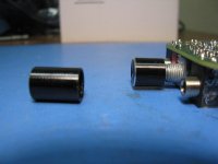
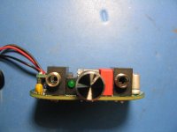
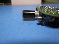
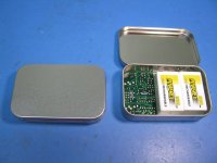
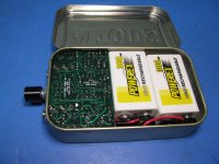
Mint tin hole cutting suggestions
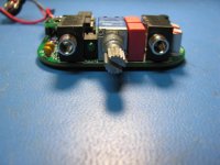
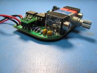
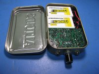
Here is the final result with the V4.1 board in the post above mounted in a mint tin. I have some mint tin hole-cutting tips.
* The first 3 photos are outside shots using the shorter (10mm) Adafruit knob. The input 3.5mm jack is on the right, looking at the mint tin end head-on. It turns out I screwed up a bit here and didn't get the holes as low as I could have. The 3.5mm jacks are up just a little from the bottom of the tin. Ideally the top of the those jacks should sit flat on the bottom of the tin. The good news though is that there is plenty of room above the board, no need to insulate the back of the board even if you mess up and mount it a little higher like this.
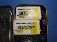
* The next next 4 photos show the fit of the batteries inside the case. This is sort of a maximum battery width situation. The 300mAHr Powerex 8.4V "9V" NiMH rechargeable batteries here are already a bit wider than regular throw-away batteries and wider than many other NiMH "9V". Then on top of that I'm using the molded battery snaps (235-M) which are wider than the vinyl (235) version. Even so the batteries still fit just fine, although one gets shifted up a bit. They are not in tight at all here, there is still 1mm of side play or so. Filing the corner of the outer molded snap slightly (or using a vinyl snap) would create even more room, if someone needed it.
There is some space between the batteries and the lid of the mint tin, so they will rattle until some foam is put on top. A good thing to consider here is Scotch double-stick mounting tape that is 3mm thick. Put a strip of that on the lid above each battery, then stick paper on the other side so they don't stick to the batteries, just press on them. That should eliminate any battery rattle.
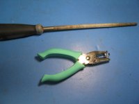
* The final photo is how I made the holes. I first placed the board inside the tin (tip it slightly to go under the edge, the board is longer than the rolled edges at the top of the tin) and used a fine point Sharpie to mark around the volume pot shaft. Then I used a standard handheld paper punch (bought it in the office supply section at Target for $1 or so) to punch an initial hole in the metal. The metal is so thin it goes right through. Then I used the rat-tail file (cat-tail? lol) rotated in the hole to enlarge it enough for the threads on the pot shaft to fit through.
Then with the pot shaft pushed partially through that center hole I just kind of eyeballed the center of the 3.5mm jacks and put a dot with the marker on the outside of the tin. Then punched those holes. Both wound up too high intially. I used the punch to punch more out of the bottom of each hole, then used the file to round the holes out and enlarge them.
Finally the nuts and washer goes on. I haven't made a hole for the LED in this one. I also haven't used the printable paper template that I've posted at the Google Drive link. Using the template should give even more precise results.
Remember that clicking on the arrows in the lower left of these photos will enlarge them.
Here is the final result with the V4.1 board in the post above mounted in a mint tin. I have some mint tin hole-cutting tips.
* The first 3 photos are outside shots using the shorter (10mm) Adafruit knob. The input 3.5mm jack is on the right, looking at the mint tin end head-on. It turns out I screwed up a bit here and didn't get the holes as low as I could have. The 3.5mm jacks are up just a little from the bottom of the tin. Ideally the top of the those jacks should sit flat on the bottom of the tin. The good news though is that there is plenty of room above the board, no need to insulate the back of the board even if you mess up and mount it a little higher like this.
* The next next 4 photos show the fit of the batteries inside the case. This is sort of a maximum battery width situation. The 300mAHr Powerex 8.4V "9V" NiMH rechargeable batteries here are already a bit wider than regular throw-away batteries and wider than many other NiMH "9V". Then on top of that I'm using the molded battery snaps (235-M) which are wider than the vinyl (235) version. Even so the batteries still fit just fine, although one gets shifted up a bit. They are not in tight at all here, there is still 1mm of side play or so. Filing the corner of the outer molded snap slightly (or using a vinyl snap) would create even more room, if someone needed it.
There is some space between the batteries and the lid of the mint tin, so they will rattle until some foam is put on top. A good thing to consider here is Scotch double-stick mounting tape that is 3mm thick. Put a strip of that on the lid above each battery, then stick paper on the other side so they don't stick to the batteries, just press on them. That should eliminate any battery rattle.
* The final photo is how I made the holes. I first placed the board inside the tin (tip it slightly to go under the edge, the board is longer than the rolled edges at the top of the tin) and used a fine point Sharpie to mark around the volume pot shaft. Then I used a standard handheld paper punch (bought it in the office supply section at Target for $1 or so) to punch an initial hole in the metal. The metal is so thin it goes right through. Then I used the rat-tail file (cat-tail? lol) rotated in the hole to enlarge it enough for the threads on the pot shaft to fit through.
Then with the pot shaft pushed partially through that center hole I just kind of eyeballed the center of the 3.5mm jacks and put a dot with the marker on the outside of the tin. Then punched those holes. Both wound up too high intially. I used the punch to punch more out of the bottom of each hole, then used the file to round the holes out and enlarge them.
Finally the nuts and washer goes on.
I haven't made a hole for the LED in this one. I also haven't used the printable paper template that I've posted at the Google Drive link. Using the template should give even more precise results.Remember that clicking on the arrows in the lower left of these photos will enlarge them.
Attachments
Last edited:
I may go with this against local traditions, but would recommend to start with LTSpice.
Yes, it looks a bit less user friendly, however it is much more powerful instrument, in my opinion. Also there is a huge online community which can help with pretty much any question.
I completely agree here, I don't like TINA a bit. Worse, the TI version is essentially freeware that wants the user to upgrade to the (paid) manufacturers version for the more important functions, as I recall. LTSpice is the way to go. For anyone using the Eagle layout editor out there, LTSpice is now part of Eagle too. You can move the schematic between the two.
Ugh. I've been busy. Taken me quite a while to get to sit down and play with TINA. Yes, I saw your advice and I actually do want to play with LTSpice sometime, but I figured right now there should be a OPA1688 spice model (macro?) for TINA and I wasn't sure how much work it would take to convert that for LTSpice.
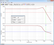
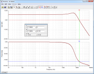
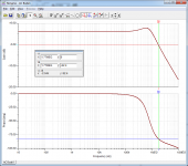
But I finally got started... And since I was just getting started, I though I'd keep it simple. I simulated the gain of 1 case using a 1k + 1k set of resistors, both with and without the 47 pF compensation cap, for loads of 16, 32, 330 and 600 Ohms. Then I tried using R1 and R2 of 825 Ohm which I think was mentioned somewhere earlier in this thread. The results are:
Code:
	R1	R2	Ccomp	Rload	Cross	Margin
Run 1	1k	1k	47pF	16r	-81.95	98.05
Run 2	1k	1k	47pF	32r	-73.07	106.93
Run 3	1k	1k	47pF	330r	-61.4	118.6
Run 4	1k	1k	47pF	600r	-60.85	119.15
Run 5	1k	1k	-	16r	-85.38	94.62
Run 6	1k	1k	-	32r	-79.43	100.57
Run 7	1k	1k	-	330r	-93.33	86.67
Run 8	1k	1k	-	600r	-98.12	81.88
Run 9	825r	825r	47pF	16r	-82.4	97.6
Run 10	825r	825r	47pF	32r	-73.88	106.12
Run 11	825r	825r	47pF	330r	-64.27	115.73
Run 12	825r	825r	47pF	600r	-63.98	116.02
Which is really nothing special since I didn't simulate the load capacitance. But like I said, just getting started. I figured I should ask here if these numbers look sensible, or have I made a mistake? I'm also open to suggestions!
Next up is to simulate the load capacitance. Would 400 pF do it? And that goes in parallel with Cload, yes?
Attachments
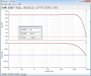
Second post to add rest of plots. I included these just because the numbers in the table don't describe that peaking at the end of the gain plot.
Attachments

* Next two are measuring the HiTech brand 7.4V nominal lithium polymer rechargeable 2-cell 720 mAhr battery. The open circuit voltage is 8.28Vdc, the voltage under load is 8.26Vdc. The current through the series setup is 8.26/159.4 = 51.8mA. The voltage across the internal battery resistance is 8.28 - 8.26 = 0.02Vdc. The internal resistance of this rechargeable battery is 0.02Vdc/51.8mA = 0.386 ohms. WOW!!
I wonder if that resistance you're measuring is mostly the pass element of the battery protection circuit. Not that it matters, that's plenty low enough.
The bad: Both the place selling the Tenergy and the one selling the HiTech cells don't ship to where I am.
Or at least their cart doesn't include it by default. I'll try dropping them both an e-mail to ask, but if not....Knob - Uh, JDS Labs has a nice one for their CMOY.
I wonder where they source it from.The latest BOM - I think there's a minor error where it says you need only 1 battery clip instead of two. I can't check it right now though, my version of Excel at home doesn't do .xlsx and it doesn't seem to want to open in Google docs either...
I might have missed it, but why do we install the board upside down? Is it just to avoid shorting out the underside against the tin?
Would 400 pF do it? And that goes in parallel with Cload, yes?
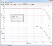
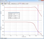
Looking good on the sims! You are right, there is some mucking around in LTSpice to add the model for a new chip to the library, then you also have to create the symbol for the part adn link the two. Fairly easy to do though. I see that Mooly has a link at the bottom of his posts with a post to LTSpice tips. I haven't looked at that, but it would probably be a good place to start when the time comes.
You have 6dB = 2x gain, just as expected. Completely flat frequency response and 0 phase shift through the audio band, for the purely resistive load. Do try 400pf in parallel with the load. It's the load capacitance that can cause things to go south from here.
The load capacitance is another area where johnc124 is doing something different than what I've done in the past. On all my other headphone amps I've used a minimum tests load of 1000pF, and on the last couple of designs raised that to 2200pF (=0.022uF). I am still sticking to that for any desktop amps because I've just seen too many posts over the years where some headphone and cable setups wind up with over 1000pF and the amp oscillates. On this particular headamp though I've decided to stay close to TI's design goals, including that 90dBSPL maximum instead of my usual 120dB SPL. Although in the "headphone SPL" folder at the Google drive link for the Super CMOY every headphone type analyzed so far will do 110dB SPL with no problem, even at the +/-7Vdc low battey cut-off point. So long story short, go with 400 or 500pF Cload since that is what johnc124 is using (I believe, from his posts).
Those are 4 good test resistance value you are using, too. They cover the vast majority of headphones and IEMs out there.
Last edited:
I wonder if that resistance you're measuring is mostly the pass element of the battery protection circuit. Not that it matters, that's plenty low enough.
No, rather amazingly the SSR mosfet "on" resistance really is 0.0125 ohms, and I've measured it! Or at least, more accurately, I've measure it with the SSR in the "AC Wired" configuration (that was how my V3.0 test board was set up) where the two SSR mosfets are in series rather than parallel. There I measured the voltage drop across the SSR (amplifier was turned on with no load), then divided that by the datasheet idle current value for the OPA1688 of 1.6mA * 2. The result was amazingly close to the datasheet 0.05 ohm "on" resistance for the Coto CT128 part. I haven't gone back and re-measured things in the current V4.0/V4.1 "DC Wired" configuration where the SSR mosfets are in parallel, but given the other result I would fully expect it to be near 0.0125R.
So there is a good test to try, if someone wants to mess with it and post the results.
Just measure the voltage drop across either SSR with the Super CMOY turned on and with no headphone load. You will need a fairly accurate DMM that can read down to 1uV = 0.001mV since the drop across the SSR will be in the 40uV range.In fact, I was having a email chat with another electrical engineer just a day or two ago about alternatively using the rather common DIP8 SSRs that have two sets of dual opto-mosfets on the chip. Those are only available with minimum "on" resistances of around 2 ohms. My thinking is that would actually be OK. Given that the battery resistance of the primary cells is 5.5 ohms and the NiMH is 2.2ohms, then we are assuming neither will matter due to the PSRR of the chip, an argument could be made than a SSR mosfet Ron of 2R wouldn't matter either. In fact that 2R plus the 2.2R in a NiMH is still less than the internal resistance of the throw-away cell. Those dual channel DIP8 jobs are quite a bit cheaper, too.
But, lol, I designed the Super CMOY to be the Lexus (Lamborghini?) of CMOYs, so 0.0125 "on" resistance it is.
The bad: Both the place selling the Tenergy and the one selling the HiTech cells don't ship to where I am.
Hmmm... I may be able to help with that. I'll PM.
Knob - Uh, JDS Labs has a nice one for their CMOY.
I just had a look. That is a nice knob! If anyone finds a source for any more 10mm-or-so diameter knobs please post.
The latest BOM - I think there's a minor error where it says you need only 1 battery clip instead of two. I can't check it right now though, my version of Excel at home doesn't do .xlsx and it doesn't seem to want to open in Google docs either...
Good find! Corrected and re-posted, along with filling in a few more Farnell resistor equivalents.
I might have missed it, but why do we install the board upside down? Is it just to avoid shorting out the underside against the tin?
That is it - by doing the upside down install it guarantees no shorts to the metal can with no insulation required. I like using the Switchcraft vertical 3.5mm jacks in projects since they preserve front panel space and are high quality jack. Those jacks turned into a made-to-order board standoff in the front.
I tend to go for some unusual mechanical designs with my stuff.
Like the O2 Booster Board that fits in the top O2 case slot and plugs into the O2 PCB. The top-slot ODAC carrier board for my ODA desktop amplifer is another. In addition to being top-slot it has a big hole cut out of the center to let the heat from the chips below pass through.
Last edited:
No, rather amazingly the SSR mosfet "on" resistance really is 0.0125 ohms, and I've measured it! Or at least, more accurately, I've measure it with the SSR in the "AC Wired" configuration (that was how my V3.0 test board was set up) where the two SSR mosfets are in series rather than parallel. There I measured the voltage drop across the SSR (amplifier was turned on with no load), then divided that by the datasheet idle current value for the OPA1688 of 1.6mA * 2. The result was amazingly close to the datasheet 0.05 ohm "on" resistance for the Coto CT128 part. I haven't gone back and re-measured things in the current V4.0/V4.1 "DC Wired" configuration where the SSR mosfets are in parallel, but given the other result I would fully expect it to be near 0.0125R.
Heh, I was wondering where those resistance numbers came from.
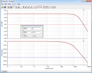
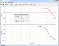
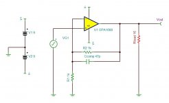
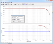
But no, I meant the battery's own internal protection circuitry. At least I assume there's one in there. Lithium chemistry batteries for end users usually have a under/over-voltage protection circuit built in that disconnects the internal cell(s) from the load/charger should things go wrong.I did some more simulations. Gain of 2x with 1k or 825 Ohm resistors, driving a capacitive load as shown in the image.
Code:
R1	R2	Ccomp	Cload	Rload	Cross		Margin

1k	1k	Nil	400pF	16r	-89.63		90.37
1k	1k	Nil	400pF	32r	-92.15		87.85
1k	1k	Nil	400pF	330r	-150.04		29.96
1k	1k	Nil	400pF	600r	-155.04		24.96

1k	1k	47pF	400pF	16r	-85.25		94.75
1k	1k	47pF	400pF	32r	-81.06		98.94
1k	1k	47pF	400pF	330r	-118.57		61.43
1k	1k	47pF	400pF	600r	-124.65		55.35

1k	1k	Nil	1nF	16r	-96.82		83.18
1k	1k	Nil	1nF	32r	-112.58		67.42
1k	1k	Nil	1nF	330r	-168.25		11.75
1k	1k	Nil	1nF	600r	-171.52		8.48

1k	1k	47pF	1nF	16r	-90.8		89.2
1k	1k	47pF	1nF	32r	-96.39		83.61
1k	1k	47pF	1nF	330r	-148.09		31.91
1k	1k	47pF	1nF	600r	-151.75		28.25


R1	R2	Ccomp	Cload	Rload	Cross		Margin

825r	825r	Nil	400pF	16r	-89.1		90.9
825r	825r	Nil	400pF	32r	-91.1		88.9
825r	825r	Nil	400pF	330r	-147.39		32.61
825r	825r	Nil	400pF	600r	-152.36		27.64

825r	825r	47pF	400pF	16r	-85.78		94.22
825r	825r	47pF	400pF	32r	-82.37		97.63
825r	825r	47pF	400pF	330r	-119.87		60.13
825r	825r	47pF	400pF	600r	-125.56		54.44

825r	825r	Nil	1nF	16r	-96.2		83.8
825r	825r	Nil	1nF	32r	-111.27		68.73
825r	825r	Nil	1nF	330r	-116.28		63.72
825r	825r	Nil	1nF	600r	-169.54		10.46

825r	825r	47pF	1nF	16r	-91.5		88.5
825r	825r	47pF	1nF	32r	-98.15		81.85
825r	825r	47pF	1nF	330r	-148.79		31.21
825r	825r	47pF	1nF	600r	-152.33		27.67
Not sure if I'm interpreting this right (or didn't make a mistake in the simulations...) but it looks like one could actually get away with not using that 47pF cap for 32 Ohm and below headphones. But it does make a difference when things get "worse".
Also, looks like using 1k/1k resistors or 825r/825r makes little if any difference to the phase margin (both combinations give a gain of 2x).
I haven't attached any of the plots, since there's a lot of them. But if anyone's interested in any in particular, let me know.
Also, I was curious, what happens if we continue to crank up the load capacitance....
Code:
R1	R2	Ccomp	Cload	Rload	Cross		Margin

1k	1k	Nil	2nF	16r	-109.72		70.28
1k	1k	Nil	2nF	32r	-136.27		43.73
1k	1k	Nil	2nF	330r	-180.24		-0.24
1k	1k	Nil	2nF	600r	-182.56		-2.56

1k	1k	47pF	2nF	16r	-101.34		78.66
1k	1k	47pF	2nF	32r	-120.82		59.18
1k	1k	47pF	2nF	330r	-165.74		14.26
1k	1k	47pF	2nF	600r	-168.22		11.78
At 330 at 600 Ohms and 2nF, that 47pF cap makes the difference between stable and unstable. Although that margin is so narrow it probably isn't a good idea anyway. I think I tried playing with larger values (220 pF?) for the feedback cap, but they didn't offer much improvement.
It is possible to measure the actual capacitance of headphones? I'm wondering what real numbers look like.
Attachments
I tend to go for some unusual mechanical designs with my stuff.
I saw that... Impressive work!
- Home
- Amplifiers
- Headphone Systems
- OPA1688 Super CMOY, 2x 9V with real ground and headphone relay - PCBs