Some good stuff happened this morning. The PCB fabrication company found a layout mistake I made during their pre-check - forgot to mirror the part numbers for the silkscreen for the parts on the back of the board - so that gives me a chance to send in a version with a few more updates.
Yeah I wouldn't be surprised a few of the O2 fabricators would be willing to build one up and/or supply a PCB or parts kit if anyone is interested. Once I get it tested I'll shoot off a PM or email to the group, including Head-n-Hifi and Audio Poutine here on the DIYA manufacturers forum. An interesting value-add would be for the outfits to populate all the SMD parts but leave the through-hole parts for the DIY builder, as an option. Some of the DIY fun but none of the SMD soldering. I've tried to leave as much stuff as through-hole as possible, in the spirit of what RocketScientist / NwAvGuy did with the O2 amp.
Looks like I messed up the Google Drive link on the Google end for the high resolution PCB pictures. They are here:
https://drive.google.com/folderview?id=0B67cJELZW-i8VmhVNk5PODNtZnc&usp=sharing in the ODA -> 80x160PCB B4 case directory -> most recent date.
Some new stuff that should make it in on this PCB fab revision:
- I've increased the number of (optional) coupling film coupling caps in the middle on each channel to 6. That is 6 * 4.7uF = 28uF now, with a very good electrical reason. With 28uF I'm able to drop that output stage input bias return resistor (the 40.2k R12 and R13 on the O2) all the way down to 5k, a decrease in Johnson / thermal noise, and still beat the high pass filter corner frequency from the O2. The O2 low end HPF is about 1.8Hz while the 6 caps and 5K resistor here would yield about 1.12Hz. That means the low end of the frequency response for the amp starts dropping at about 10Hz on the O2, where here is would be at about 5Hz. The extra margin here also takes into account that each of those caps is 20% tolerance in value, in case someone gets the luck of the draw and the 20% is all on the low end for each.
The problem is cost! 6 x 4.7uF Wima film caps is about $25 per channel just for the coupling caps, or $50 total for both channels. Aarrgghh. So this is all optional - all those caps are in parallel on each channel. Instead just one 4.7uF coupling cap can be used / populated per channel ($4.50 each) with a 10K resistor (if using the 1K pot) or a 40.2K resistor like the O2 (if using a 10K pot). The HPF corner frequency would still slightly beat the O2 since RS used 2.2uF caps. Then later on as money permits all those remaining parallel film caps could optionally be soldered in and the two resistors changed to the lower values to take advantage of the lower (than the O2 amp) thermal noise.
- ·The headphone relay circuit now has its own small 24Vdc supply from a MC78L24G, the 40V input On Semiconductor version of the TO-92 regulator. This solves a problem caused by the variable voltage power supply rails of the amplifier, which would cause variable turn-on delay times with the relay control circuit. The constant 24Vdc supply provides a fixed time delay. The 24Vdc relay coil only pulls about 8mA, well within the specs for the 100mA 500mW regulator chip.
- · The number of power supply voltage choices are reduced to 2 from 3, +/-7Vdc and +/-17Vdc (or any two voltage levels, just set by the LDO resistors that are picked). The reason is a lack of right angle PC mount DP3T switches available at Mouser and Digikey. DPDT is the best I could find that would fit in the space available. An external panel-mounted rotary switch could always be used instead to give more power supply voltage choices. +/-7Vdc should cover most headphones below 80 ohms while +/- 17Vdc should cover most above 80R. Those power supply voltage levels are resistor-settable anywhere in the 5Vdc to 17Vdc range, thanks to the adjustable voltage regulators (and heat sinking!), so instead the switch could be wired up for +/-12Vdc and +/-15Vdc power supply rails, etc.
- Beefed up the headphone output relay to 3A DC contacts (2A AC).
Attachments
Last edited:
Glad to see that O2 got some sort of logical successor. Also glad to see that it moves toward more sophisticated design. Despite that O2 truly served its purpose, as for my taste it needed some extra touch on the schematic side. Using several tricks it was easy to improve distortion performance, even without adding extra active components.
To encourage author of ODA, will drop my fraction of substance on low distortion fan blades
Here is a few pictures of my DAC with onboard headphone amplifier. It is sort of less universal thing that ODA. It has fixed gain and no extra frequency compensation stuff, but it was built for very particular purpose.
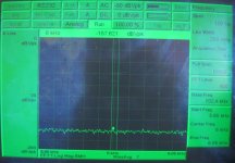
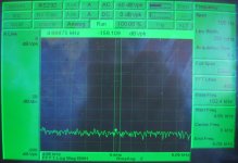
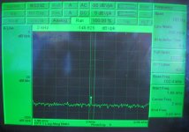
There are also few pictures with distortion measurement results. On these photos you can see distortion products of 1k tone, amplitude 3Vpk (~+9dBVpk) driven onto 15Ohm resistive load. Because of measurement technique harmonics are actually attenuated by 6dB. So as a result you need to add 3dB to number you see on the screen to get harmonic level in relation to the main 1kHz tone. It comes to around -149dB for the second harmonic, -153dB for the third and more that -162dB for the forth one.
To encourage author of ODA, will drop my fraction of substance on low distortion fan blades
Here is a few pictures of my DAC with onboard headphone amplifier. It is sort of less universal thing that ODA. It has fixed gain and no extra frequency compensation stuff, but it was built for very particular purpose.
There are also few pictures with distortion measurement results. On these photos you can see distortion products of 1k tone, amplitude 3Vpk (~+9dBVpk) driven onto 15Ohm resistive load. Because of measurement technique harmonics are actually attenuated by 6dB. So as a result you need to add 3dB to number you see on the screen to get harmonic level in relation to the main 1kHz tone. It comes to around -149dB for the second harmonic, -153dB for the third and more that -162dB for the forth one.
Attachments
Sergey888 - that is a nice looking PC board and some great results! Double sided, too. Looks like you are using a TPA6120A2 for the headphone chip.
Yeah I have come to appreciate how much performance RocketScientst / NwAvGuy managed to pack into that small space for just $30. It has been kind of a puzzle trying to figure out what could be added to it in any way that the O2 didn't already have. Finally settled on higher rail voltage, more output current, lower DC offset, and additional jacks.
Yeah I have come to appreciate how much performance RocketScientst / NwAvGuy managed to pack into that small space for just $30.
It has been kind of a puzzle trying to figure out what could be added to it in any way that the O2 didn't already have. Finally settled on higher rail voltage, more output current, lower DC offset, and additional jacks.The PCB is actually 4-layer one. It was next to impossible to resolve routing of some sections with my space restrictions. Yeah, it has TPA6120 in it, but it would not be capable to deliver this level of performance itself. I ended up with some sort of composite amp with multipole compensation.
Some ideas with O2 improvement were actually on the surface, and you picked up some of them. It certainly would not cost much (just few extra passives) to add nested feedback around output, like you did in your project. Also adding a bit of driving capabilities may help to reduce higher order crossover distortion (heavy loaded opamp tend to have these).
Anyway nice to see some good ideas been implemented.
Cheers
I agree on the 4-layer board. I'm going to try to do the final run as 4 layer. I want to use one layer as a full ground plane, single point grounded with no signal currents going through it, and one for routing. I've had to use wire jumpers in a couple of spots with just the two layers to resolve some routing issues. Those would go away with the 3rd layer. I could also keep high impedance and large signal lines a bit further apart by doing a bit of routing on the 3rd layer.
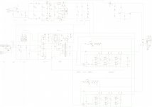
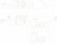
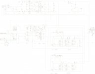
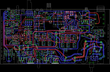
Hey I'm open to circuit and layout suggestions! Please post any thoughts. The current schematic below. I may or may not to use them, but I'll certainly take a look at any suggestions. Any distortion reduction and/or compensation circuit ideas would be especially interesting.
Speaking of compensation, I don't think I've posted that I did eventually get the very first circuit in this thread to oscillate with additional output capacitance and long cables, the OPA627 wrapped around two NJM4556A buffers in parallel. Looking into that further I found that in addition to the 100 degrees of phase lag the OPA627 has up to 1Mhz (datasheet gain/phase plot), the NJM4556A has an additional 30 degrees of lag up through 30kHz (-130 degrees, still OK). Which unfortunately then falls off a cliff and goes down to around -80 degrees at about 110kHz. That leaves zero phase margin at 110kHz, -100 - 80 = -180 = oscillation, and into the magic 20 degree phase margin buffer zone at about 90kHz. The oscillation on one channel was 77kHz and the other 80kHz. Sometimes the math actually works out.
If I had continued to use the OPA627 I would have added some phase lead compensation at the inputs to move the phase shift back into the stable zone. The BUF634 appears to have 0 degrees of phase shift up through 1mHz, from my read of the datasheet graph, which is why all those OPA627 + BUF634 amplifiers out there apparently never ran into an oscillation problem. RocketScientist avoided the problem by having the NJM4556A's not in a loop with anything else.
The good news is that so far I've had zero oscillation problems with the LME49990s substituted for the OPA627 on that same board (SOIC adapter), which tells me the phase lag of the LME49990 must be less, or possibly even phase lead. Unfortunately the gain/phase plot is missing from the LME49990 datasheet. I've sent a request into TI for that plot, but failing that maybe I can extract it myself with some measurements. It would be nice to know for certain, upfront.
Two new things on the current layout. The on/off switch is now DPDT with the relay coil looped through the extra set of contacts. That provides immediate disconnect for the headphones when the power is switched off. No waiting for power supply rails to start collapsing to disconnect the headphones. And I realized that with the DC servos the coupling caps (all $50 worth of them!) could actually be completely bypassed/jumpered and the amp run as purely DC coupled. Now there is something that couldn't (safely) be done with the O2 amplifier. The servos have a very long filter insertion delay, about 3 seconds, since they are designed to fine-tune the DC offset which is already low. But the amp has the 12 second power-on headphone relay delay, and the servos are looped back before the relay contacts, so as long as the source is turned on and plugged into the ODA input when the ODA power is switched on the servos would settle in time to null out a reasonable amount of DC on the ODA input. I also forgot to say in my last update post why the beefier relay contacts. They are for fault conditions, especially the TRS jack shorting with plugging or unplugging. The ODA output stage can probably push the better part of an amp for an instant before the current limiting kicks in, enough to weld relay contacts that are not rated properly.
Hey I'm open to circuit and layout suggestions!
Please post any thoughts. The current schematic below. I may or may not to use them, but I'll certainly take a look at any suggestions. Any distortion reduction and/or compensation circuit ideas would be especially interesting. Speaking of compensation, I don't think I've posted that I did eventually get the very first circuit in this thread to oscillate with additional output capacitance and long cables, the OPA627 wrapped around two NJM4556A buffers in parallel. Looking into that further I found that in addition to the 100 degrees of phase lag the OPA627 has up to 1Mhz (datasheet gain/phase plot), the NJM4556A has an additional 30 degrees of lag up through 30kHz (-130 degrees, still OK). Which unfortunately then falls off a cliff and goes down to around -80 degrees at about 110kHz. That leaves zero phase margin at 110kHz, -100 - 80 = -180 = oscillation, and into the magic 20 degree phase margin buffer zone at about 90kHz. The oscillation on one channel was 77kHz and the other 80kHz. Sometimes the math actually works out.
If I had continued to use the OPA627 I would have added some phase lead compensation at the inputs to move the phase shift back into the stable zone. The BUF634 appears to have 0 degrees of phase shift up through 1mHz, from my read of the datasheet graph, which is why all those OPA627 + BUF634 amplifiers out there apparently never ran into an oscillation problem. RocketScientist avoided the problem by having the NJM4556A's not in a loop with anything else.
The good news is that so far I've had zero oscillation problems with the LME49990s substituted for the OPA627 on that same board (SOIC adapter), which tells me the phase lag of the LME49990 must be less, or possibly even phase lead. Unfortunately the gain/phase plot is missing from the LME49990 datasheet. I've sent a request into TI for that plot, but failing that maybe I can extract it myself with some measurements. It would be nice to know for certain, upfront.
Two new things on the current layout. The on/off switch is now DPDT with the relay coil looped through the extra set of contacts. That provides immediate disconnect for the headphones when the power is switched off. No waiting for power supply rails to start collapsing to disconnect the headphones. And I realized that with the DC servos the coupling caps (all $50 worth of them!) could actually be completely bypassed/jumpered and the amp run as purely DC coupled. Now there is something that couldn't (safely) be done with the O2 amplifier. The servos have a very long filter insertion delay, about 3 seconds, since they are designed to fine-tune the DC offset which is already low. But the amp has the 12 second power-on headphone relay delay, and the servos are looped back before the relay contacts, so as long as the source is turned on and plugged into the ODA input when the ODA power is switched on the servos would settle in time to null out a reasonable amount of DC on the ODA input. I also forgot to say in my last update post why the beefier relay contacts. They are for fault conditions, especially the TRS jack shorting with plugging or unplugging. The ODA output stage can probably push the better part of an amp for an instant before the current limiting kicks in, enough to weld relay contacts that are not rated properly.
Attachments
Last edited:
For my opinion single point grounding may be sub-optimal in this situation, if I understand right what you mean. Nevertheless you certainly need to cut some slots in ground plane.
There are only to places where you will have significant ground currents. It is the fraction of plane from power inlet to main capacitors in PSU (the scariest one, will contain a lot of 50Hz products), and from these capacitors to output connector. You just need to make sure that these currents will not upset low signal part of your design.
Speaking of oscillation. You may consider having and output Zobel network with series inductor.
Cable, as an output load, may affect stability as a extra capacitor, or like unterminated transition line. In both cases you want to have something isolating amp output from load on higher frequencies.
Speaking of oscillation. You may consider having and output Zobel network with series inductor.
Good suggestion! I'll do it. I'll add pads for a zobel at the output, which can then be optionally populated if needed.
Something unrelated, I was sent a link yesterday to RocketScientist / NwAvGuy's listing on his blog from back in November of 2011 about what he was thinking of for the ODA at the time:
NwAvGuy: Objective Desktop Amp (ODA) & DAC
I had forgotten about that listing. Looks like I've hit a lot of it except the inclusion of surface mount parts. The total parts cost is higher though, and yes this one is in fact capable of spot-welding with the high output current capability.
I improved the power supply in a different way by adding more physical space around the noisy AC parts and adding the second let of low noise regulators. I know from some email along the way he was thinking of an on-board AC PCB mount transformer, but later in a blog comment saw that he was unable to find any here in the US that didn't make an audible buzz. Running the wall AC to the unit gets into UL and CSA certification land, which is why I stayed with the wall wart and half wave supply. The wall wart is certified so the ODA doesn't have to be.
Last edited:
Good call with safety. All you circuitry in this case can be classified as SELV, so as far as power plug has double or reinforced insulation, amplifier will be literally IEC60950 compliant
As for possible pick up of noise from AC part. There is a general approach which may help. Because frequency of our interest is quite low, all coupling from AC power supply lines (and actually from DC supply lines as well, they consist rectified component of amplifier output current) to signal lines will be mostly inductive. To reduce this effect, beside quite obvious spacing, you want to keep area of return current loops as small as possible, on both sides. In this case having ground planes helps. This way (moving apart, reducing areas) you decrease mutual inductance of nets that may possibly interact.
Having extra layer of voltage regulation may not bring as much improvement. But there is something that I would recommend to do. To eliminate possible coupling of the front end amplifiers and what called in this case, output stage, I would put an extra RC filtering on front end opamp supply lines. Another way of doing this is powering them up from separate regulator. For example you can supply voltage to output stage from the LM317/337, and than use extra regulators to power up the input opamps.
You also mentioned that in one case you had to use phase lead compensation. In addition to that, if this one "is not strong enough" you can create additional second order roll off around first op amp. This way it is easy to compensate it even for gain of +1.
The Gerbers on this project finally went out to fab last night. They tell me the files passed DRC and are now off to the factory.
Some final new stuff:
* Added an input select switch to switch between the rear RCA jack and front 3.5mm jack. Sources can be left plugged into both.
* Added another set of RF filter parts to the rear RCA jacks due to the new switch. Moved the external input connection PCB holes to the back RCA jack (for the ODA connection or other external input)
* Added the Zobel nework on each channel that Sergey888 suggested. Populating the parts is optional, of course.
* Added parallel traces in a couple of places for additional current capacity (buffer output lines, voltage regulator) where the trace width was confined by pin spacing.
I give up on Google drive for now. Apparently I need to convert the sharing link to a permalink, but that doesn't work for folders. Once I get it figured out I'll repost a link to the high resolution stuff, including the Gerber zip file. The low rez stuff is below.
Attachments
Sergey888 - good suggestions! I think you are right about the ground plane just in the AC area. I hadn't thought about that. I usually avoid ground planes to know exactly how the currents will flow, but you are right, in the AC high current area who cares. Shortest route is best. I'll probably adopt that on any future revision. I'll make a small ground plane polygon in that area.
I actually did have a separate set of voltage regulators for the gain stage at one point but removed them. Hmm.... I may take a second look at that on future revisions. May not help CMRR but there may be some other isolation benefits.
I agree that any decreased ripple and noise from the two sets of regulators (vs. just one set) are probably going to be useless. RocketScientist measured noise floor with his dScope and found that bettering the LM7812s didn't make any difference with the O2 amp. Opc has posted the same about his Wire amp and the LM317/337s with the audio precision measurement.
But in this case something has to be added before the LT1963A anyway to drop voltage since that part is just 20V max input while the LT3015 is 30V, combined with a +/-17Vdc output voltage target. I've had a BC139 based stage fed by a LED or zener in there on various revisions, but everytime I added that I realized that with 1 more resistor and 2 caps I could just add the regulator. Then there is the issue of spreading the dissipation out, which became more important with the variable voltage rails. At +/-7Vdc rails the LT parts will be dissipating a fair amount of power. The LM parts can dissipate the rest, especially if a 24Vac transformer is used.
Then finally I know that jackinnj on the forum here posted that he has done some blind tests with various voltage regulators in the same audio circuit and found that the LT1963A/LT3015 regulators generally won in listening tests. I'm just curious.
qusp - One interesting thing is these X2Y EMI caps seems to essentially be working on common mode noise between the input lines, at least for higher frequency EMI. I've left some pads for them and am kind of curious to give those a try.
Last edited:
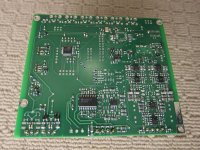
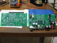
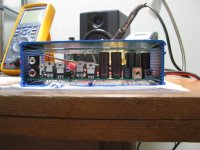
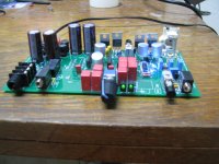
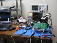
I've received the first batch of test PC boards for this project back *already* - just 8 days total from submission to IteadStudio and DHL shipping from China back to me in the US! Pretty amazing. I've partially stuffed one last night, pictures below, and tested out the power supply section. Works so far!
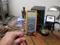
From the pictures below, -6.94Vdc and +7.01Vdc in the "low" power rail switch position and +/-16.9Vdc in the other. This weekend I'll do half load (350mA per regulator) and full load (700mA per regulator) tests with a scope to look at pre-regulator vs.final regulator output ripple and noise.
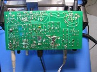
The surface mount soldering so far hasn't been too difficult. I soldered in the SOIC14 clipping indicator chip (TL064), both LME49990 gain stage chips (one of the bottom of the board) and several of the 1206 resistors and caps on the top and bottom. The build work is definitely a step up in DIY challenge from the O2 with the surface mount stuff. If you don't have a lot of surface mount soldering experience you will be better with it by the time you are done with this board. Just get a good pair of tweezers, a panavise to hold the board and free a hand, and a magnifying glass on a stand. Then grip the part with the tweezers, line up the part with the pads and tack solder one end of each part (or one leg of each IC) first (solder already on the tip). Then go back and solder the rest of the part and touch up the tacked end.
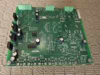
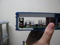
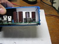
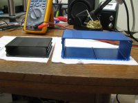
The first two pictures show the size difference between the standard O2 amplifier B2-080 case and the new B4-080 ODA case, and the PCB. The next 2 photos shows something I wanted to correct from the O2, not enough space between the circuitry and box edges (and metal case parts under the board). This one has gobs of space. I may have overdone it, in fact, and may scoot that in a mm or two in the next board turn.
The next photo shows that the caps and other parts on the PCB do clear a PC board inserted into the top case slot, allowing for an "accessory board" up there with more stuff and/or and ODAC. I just slid in another one of these PC boards for now to show the spacing. The B4-080 case actually has more space from the top PCB to the top of the box than from the bottom PCB to the case bottom.
From the pictures below, -6.94Vdc and +7.01Vdc in the "low" power rail switch position and +/-16.9Vdc in the other. This weekend I'll do half load (350mA per regulator) and full load (700mA per regulator) tests with a scope to look at pre-regulator vs.final regulator output ripple and noise.
The surface mount soldering so far hasn't been too difficult. I soldered in the SOIC14 clipping indicator chip (TL064), both LME49990 gain stage chips (one of the bottom of the board) and several of the 1206 resistors and caps on the top and bottom. The build work is definitely a step up in DIY challenge from the O2 with the surface mount stuff. If you don't have a lot of surface mount soldering experience you will be better with it by the time you are done with this board.
Just get a good pair of tweezers, a panavise to hold the board and free a hand, and a magnifying glass on a stand. Then grip the part with the tweezers, line up the part with the pads and tack solder one end of each part (or one leg of each IC) first (solder already on the tip). Then go back and solder the rest of the part and touch up the tacked end.The first two pictures show the size difference between the standard O2 amplifier B2-080 case and the new B4-080 ODA case, and the PCB. The next 2 photos shows something I wanted to correct from the O2, not enough space between the circuitry and box edges (and metal case parts under the board). This one has gobs of space. I may have overdone it, in fact, and may scoot that in a mm or two in the next board turn.
The next photo shows that the caps and other parts on the PCB do clear a PC board inserted into the top case slot, allowing for an "accessory board" up there with more stuff and/or and ODAC. I just slid in another one of these PC boards for now to show the spacing. The B4-080 case actually has more space from the top PCB to the top of the box than from the bottom PCB to the case bottom.
Attachments
Last edited:
Wow looks like a great start. I really like the blue aluminum enclosure. Maybe that can be something to distinguish it visually from the o2, although I'm sure people will use whatever color they want. I almost bought a micromega myzik amp but I stayed strong and will keep the faith and wait for a commercial version of this. Hopefully by 2014
edit: I'm a moron, I just realized o2 is oxygen.. did rocketscientist call it that because it adds airiness to the soundstage? I know he's all about transparency. maybe since yours is blue it can be the h20
edit: I'm a moron, I just realized o2 is oxygen.. did rocketscientist call it that because it adds airiness to the soundstage? I know he's all about transparency. maybe since yours is blue it can be the h20
Last edited:
I really like the blue aluminum enclosure.
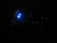
Turns out that the insides are blue right now, too!
I had used two blue chip LEDs to set the upper and lower window comparator voltage levels for the clipping detect circuit. I thought that I had picked a series resistor value that wouldn't put out much light, but looks like I missed the mark, photos below. It really blasts blue! Those are going to have to change to zeners anyway since the output stage stays further away from the the rails than 2V. But still kind of funny, it looks like one of those PC cases that use the blue cold cathode lighting inside the case.Attachments
Well here is an update on this ODA project. I have sound coming out and all I can say is wow! I really have to give RocketScientist / NwAvGuy credit on his design philosophy and choice of parts. Really produces some stunning sound.
But there are a few catches, details below, most notably the LME49990 output stage chips are going away. At this point I feel confident enough in the results not to need another board spin to post the Gerbers. I'm having to fix a few minor layout issues and I should have the BOM, Gerbers, and build instructions including the various options on the build out posted within a couple of weeks.
The 50% attenuation resistor, 1K pot, and reduced 5K ground return resistor on the output stage are huge successes, as is the dual voltage power supply. All are doing exactly what I wanted them to do. With the 1K attenuation resistor in series with the 1K pot the pot is now roughly at the 2:00 position with all of my "hot" (2V or more sources) sources and 1x gain, which is great. No more pot that is only 1/4 of the way up at 1x gain.
In the build instructions I'm including a full writeup on chosing the gain resistors and the interaction with the optional attentuation resistor. But note that a set of gain resistors that produce 1x, 2x, 4x, and 6x with no attenuation resistor will produce 1/2x, 1x, 2x, and 3x with a 50% attenuation resistor installed. That is how mine is wired and it is *fantastic*, for those of us with hot sources. Those are just the right levels.
The 1/2x level seems like kind of a waste at first blush,, running the signal through a 1x amp stage which will add a tiny bit of noise, then cutting it in half with a resistor divider. But what you are getting is effectively an impedance converter. The ODA input impedance is still 10K, to not load an ODAC or other source requiring high impedance, but the first stage output is the 1K pot and 1K attentuation resistor for lower Johnson / thermal noise. The lower 1K pot value vs. the 10K in the O2 seems to have worked - I hear just zero audible background noise even with the highest gain resistor bumped up to 12x.
The two attentuation resistors are full sized 6mm "low noise" resistors given the higher current now through the 1K pot. The Johnson / thermal noise is just a function of resistance value and ambient temperature. But the current noise can be improved upon somewhat by resistor design, so here is one of those places where a "low (current) noise" resistor has some value.
Related to the pot, the 4.99K ground return resistor (vs. 40.2K in the O2) is working exactly as expected. With the LME49990 output stage and DC servo completely bypassed, so that the coupling cap output is going right to the parallel buffer inputs (as in the O2), I'm getting just 1.4mV DC offset on one channel and 1.1mV on the other. That is pretty amazing given that the O2 is around 3mV and here we are pulling 3x the input bias current through the resistor with 3 output chips per channel vs. one. But the math works as it should, the 40.2K / 5K resistor reduction reduces the voltage drop that gets reflected back to the buffer outputs, along with further decreasing Johnson noise from the 5K vs. 40.2K resistor.
The LME49990 gain stage is working well. Stable and was easier to solder the SMD chips than I expected.
I forgot to include a compensation capacitor from the output of the output stage LME49990 chips back to the non inverting input to clip the bandwidth a bit, with the result of the two chips oscillating at about 330kHz each as laid out. Adding a 2200pF cap to each chip solves the problem, but I've since decided this output stage loop is just not a good idea here. The buffer chips are vastly slower than the LME49990, which is a cart-before-horse situation. There is a chance that just the right capacitive load could throw the loop into oscillation. Some types of headphones are primarily capacitive. RocketScientist / NwAvGuy found from his tests that the NJM4556As by themselves were unconditionally stable with any capacitive load. Given the quality of the sound I'm hearing with the buffer chips fed directly, I'm going to err on the side of stability and eliminate the LME49990s in the output stage.
The NJM4556AL chips being full fledged op-amps that don't require being in a loop with anything else, as opposed to purely a buffer chip with high Vos that must be placed in a loop like the LME49600 or BUF634, is also a feature that I really should be taking advantage of (as with the O2 amp) to reduce parts count. Since my #1 improvement goal with the O2 output stage was reduced DC output offset, I'm already half way there with the 5K input bias return resistors now reducing offset to 1.1 - 1.4mV. The DC servo circuit should do the rest.
The DC servo circuit has a big challenge of its own though, namely that I didn't notice the SOIC8 version of the chip that I laid out is not available for sale yet. Only the smaller DGK version. TI lists the SOIC as in "preview" status, available Real Soon Now. Rather than having to solder those super small DGK packages I'm going to change the DC servo circuit to use the dual part, the OPA2188 which is currently available in SOIC8. Due to my screw-up here I have not been able to test the DC servo circuit yet. I'm going to solder a dual OPA2188 on a DIP adapter board and do some hard wiring to the PC board to test the circuit.
The DC servo circuit is currently laid out as a non-inverting servo to feed back into the output LME49990 chip. That will change to an inverting servo to feed into the buffer input, with the output LME49990 removed.
And finally the dual voltage power supply does exactly what I expected. The low voltage position transfers the heat dissipation load to the heat-sinked voltage regulators while the high voltage position transfer the dissipation load to the output buffers. The low voltage position provides the lowest power dissipation for headphones or speakers needing lower voltage swings and/or higher currents. The higher 17V position is best for high impedance 300R+ headphones. Changing the voltage switch position does not produce any audible noise at all, since I have the switch just placing a resistor in parallel with an existing resistor in the regulator circuit.
I really have to give RocketScientist / NwAvGuy credit on his design philosophy and choice of parts. Really produces some stunning sound.But there are a few catches, details below, most notably the LME49990 output stage chips are going away. At this point I feel confident enough in the results not to need another board spin to post the Gerbers. I'm having to fix a few minor layout issues and I should have the BOM, Gerbers, and build instructions including the various options on the build out posted within a couple of weeks.
The 50% attenuation resistor, 1K pot, and reduced 5K ground return resistor on the output stage are huge successes, as is the dual voltage power supply. All are doing exactly what I wanted them to do. With the 1K attenuation resistor in series with the 1K pot the pot is now roughly at the 2:00 position with all of my "hot" (2V or more sources) sources and 1x gain, which is great. No more pot that is only 1/4 of the way up at 1x gain.
In the build instructions I'm including a full writeup on chosing the gain resistors and the interaction with the optional attentuation resistor. But note that a set of gain resistors that produce 1x, 2x, 4x, and 6x with no attenuation resistor will produce 1/2x, 1x, 2x, and 3x with a 50% attenuation resistor installed. That is how mine is wired and it is *fantastic*, for those of us with hot sources.
Those are just the right levels.The 1/2x level seems like kind of a waste at first blush,, running the signal through a 1x amp stage which will add a tiny bit of noise, then cutting it in half with a resistor divider. But what you are getting is effectively an impedance converter. The ODA input impedance is still 10K, to not load an ODAC or other source requiring high impedance, but the first stage output is the 1K pot and 1K attentuation resistor for lower Johnson / thermal noise. The lower 1K pot value vs. the 10K in the O2 seems to have worked - I hear just zero audible background noise even with the highest gain resistor bumped up to 12x.
The two attentuation resistors are full sized 6mm "low noise" resistors given the higher current now through the 1K pot. The Johnson / thermal noise is just a function of resistance value and ambient temperature. But the current noise can be improved upon somewhat by resistor design, so here is one of those places where a "low (current) noise" resistor has some value.
Related to the pot, the 4.99K ground return resistor (vs. 40.2K in the O2) is working exactly as expected. With the LME49990 output stage and DC servo completely bypassed, so that the coupling cap output is going right to the parallel buffer inputs (as in the O2), I'm getting just 1.4mV DC offset on one channel and 1.1mV on the other. That is pretty amazing given that the O2 is around 3mV and here we are pulling 3x the input bias current through the resistor with 3 output chips per channel vs. one. But the math works as it should, the 40.2K / 5K resistor reduction reduces the voltage drop that gets reflected back to the buffer outputs, along with further decreasing Johnson noise from the 5K vs. 40.2K resistor.
The LME49990 gain stage is working well. Stable and was easier to solder the SMD chips than I expected.
I forgot to include a compensation capacitor from the output of the output stage LME49990 chips back to the non inverting input to clip the bandwidth a bit, with the result of the two chips oscillating at about 330kHz each as laid out. Adding a 2200pF cap to each chip solves the problem, but I've since decided this output stage loop is just not a good idea here. The buffer chips are vastly slower than the LME49990, which is a cart-before-horse situation. There is a chance that just the right capacitive load could throw the loop into oscillation. Some types of headphones are primarily capacitive. RocketScientist / NwAvGuy found from his tests that the NJM4556As by themselves were unconditionally stable with any capacitive load. Given the quality of the sound I'm hearing with the buffer chips fed directly, I'm going to err on the side of stability and eliminate the LME49990s in the output stage.
The NJM4556AL chips being full fledged op-amps that don't require being in a loop with anything else, as opposed to purely a buffer chip with high Vos that must be placed in a loop like the LME49600 or BUF634, is also a feature that I really should be taking advantage of (as with the O2 amp) to reduce parts count. Since my #1 improvement goal with the O2 output stage was reduced DC output offset, I'm already half way there with the 5K input bias return resistors now reducing offset to 1.1 - 1.4mV. The DC servo circuit should do the rest.
The DC servo circuit has a big challenge of its own though, namely that I didn't notice the SOIC8 version of the chip that I laid out is not available for sale yet.
Only the smaller DGK version. TI lists the SOIC as in "preview" status, available Real Soon Now. Rather than having to solder those super small DGK packages I'm going to change the DC servo circuit to use the dual part, the OPA2188 which is currently available in SOIC8. Due to my screw-up here I have not been able to test the DC servo circuit yet. I'm going to solder a dual OPA2188 on a DIP adapter board and do some hard wiring to the PC board to test the circuit.The DC servo circuit is currently laid out as a non-inverting servo to feed back into the output LME49990 chip. That will change to an inverting servo to feed into the buffer input, with the output LME49990 removed.
And finally the dual voltage power supply does exactly what I expected. The low voltage position transfers the heat dissipation load to the heat-sinked voltage regulators while the high voltage position transfer the dissipation load to the output buffers. The low voltage position provides the lowest power dissipation for headphones or speakers needing lower voltage swings and/or higher currents. The higher 17V position is best for high impedance 300R+ headphones. Changing the voltage switch position does not produce any audible noise at all, since I have the switch just placing a resistor in parallel with an existing resistor in the regulator circuit.
Last edited:
...I forgot to include a compensation capacitor from the output of the output stage LME49990 chips back to the non inverting input to clip the bandwidth a bit, with the result of the two chips oscillating at about 330kHz each as laid out...
Out of curiosity-
What happens in such a case? LME49990 chips get hotter due to lack of compensation cap.? Does this affects the JRC4556 performance (as its bandwith is limited to 100KHz). And finally does the HF oscillations shows any effects on loads (dummy resistive load or h/p specifically)?
Last edited:
....edit: I'm a moron, I just realized o2 is oxygen.. did rocketscientist call it that because it adds airiness to the soundstage? I know he's all about transparency. maybe since yours is blue it can be the h20
According to NwAvGuy: O2 Headphone Amp the reason for naming it Objective2 a.k.a. O2
"STALE AIR: In my experience most headphone amps (and headphone DACs) fail the accuracy, or cost, criteria above. Many have a 10 ohm or higher output impedance (QRV09, FiiO E9) while others lack enough output for popular headphones (FiiO E5, E7, Mini3) And some have excessive distortion (Mini3, NuForce uDAC-2). Some have poor transient response and/or are borderline unstable (QRV09, Mini3). Amazingly, a $39 Cmoy came closest to the above goals but it still had some serious fatal flaws—especially when configured with typical gain and into low impedance loads.
FRESH AIR: The Objective2 a conventional 2 channel amp, with 2 batteries, hence the “2” in the name. But O2 also represents oxygen, and in some ways, this amp is a breath of fresh air. It has none of the limitations listed above. It simply does a very credible job of disappearing from the signal chain leaving just the music as the recording engineering intended. Some might call it “straight wire with gain”. It’s all about accuracy but not in the usual expensive audiophile overkill sort of way."
BTW H2O would be a nice name as its the second most important element after air (O2) the first element.
Last edited:
Out of curiosity- What happens in such a case?
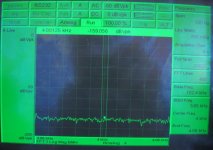
None of the chips heated up since the oscillation amplitude was only about 1V. Other than watching it on the scope the only other indication was the output DC offset voltage rising from 1mV up to 14 - 20mV. That offset level was just the 100kHz-bandwith DMM doing its best to extract a DC average out of the 330kHz wave. Since the output chips compensation drops off at 100kHz the net effect was the oscillation wave showing up as a triangle waveform with reduced amplitude.
All of this is why it is so important to get the circuit design correct. A circuit can be oscillating without giving any outside audible or visible (or heating) indication. I never tried listening to it with the oscillation happening, but there would probably not be much of a difference. The headphone driver intertia probably couldn't even begin to keep up at 330kHz.
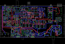
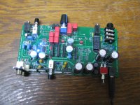
Not having better power supply bypassing on those output LME49990s was likely a big part of the oscillation. I only bypassed them rail-to-rail, not rail-to-ground. In this case that would matter since the input is ground referenced. I'm in the process of correcting that, latest layout below, for the remaining OPA2188 servo chip, using the space where the LME49990s were to add additional power supply bypass caps. That is another reason I gave up on the output LME49990s. There is just no room to add more bypass caps and keep those chips is place. The design would have to go to the 2-PCB thing with the power supply on one board and the amp parts on the other.
Another screwy oscillation thing showed up with the output LME49990s that had me puzzled for awhile. When I turned the volume control all the way down (which is on the *other side* of the DC blocking capacitors) the output DC offset shot up to 20mV with additional oscillation. At first I figured it was something to do with leakage current through all those paralleled caps.
But I eventually realized that all those caps sticking up in the air represent a fairly large surface area - an antenna, essentially - hooked right into a 110Mhz capable amplfier. I had built a radio!
When the volume control was turned all the way down that grounded one side of the paralleled capacitors, essentially grounding one side of the dipole antenna. Then the other dipole (other side of the paralleled cap plates) went right into the 110mHz LME49990. In other words, another 270R + 220pF to ground low-pass filter would be needed on the input to the output stage LME49990s to prevent them from amplifying RF pickup by those paralleled caps. Aarrggh. The joys of using high speed parts.The photos below show the board under test. In the latest layout some new stuff:
* The two input power supply filter caps are now 1000uF instead of 820uF just because they would fit. Reduces the ripple a little.
* The two inductors are now 2.8amp rated to handle full sine wave testing at full output power. The two previous ones were rated at 1.4A which covered any normal "music power" listening. Unlike RocketScientist I tend to have all the parts rated for continuous sine wave testing. Overkill for normal listening but provides excellent reliability.
* Mouser had the can sizes of the 390uF 25V organic polymer filter caps listed as 6mm diameter when they are actually 10mm. That is why they have grown bigger on the board. Luckily still enough space to accomodate them. On the current board I have the caps sticking up about 1/2 inch on their leads to clear the surrounding parts.
* Output LME49990s and OPA188s gone, replaced by a single dual OPA2188 and more power supply bypassing.
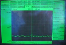
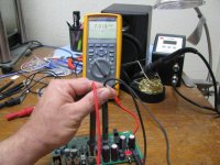
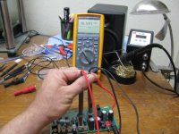
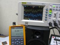
The second photo below is with the output LME49990's bypassed. The output of the paralleled capacitors right into the NJM4556AL buffers on each channel. Note on the DMM that is just 90uV of DC offset under music conditions! No DC servo yet, just the results of the paralleled output buffer chips. 57mV of AC is full volume for my AKG-K550s.
Attachments
Last edited:
- Home
- Amplifiers
- Headphone Systems
- A version of an O2 Desktop Amp (ODA)