Switch S1 has six legs. Part # is same
as BOM. Does it get modified or is it wrong.
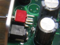
Whoops! That is the right switch, but looking through the build instructions just now I forgot to include the need to clip off the top two leads. I've attached a photo below. Just snip them off with regular wire cutter pliers. Best not to use flush cut pliers though since those leads are fairly large and could damage flush cutters.
The issue that came up with the switch was that just a DPST was needed (4 terminals), but it turns out those are rare in a right angle PC mount version, plus the DPSTs are priced about the same as the much more common DPDTs. So I went with a readily-available DPDT and just clipped two of the leads.
I'll make that change to the build instructions and re-post them in a few days. Thanks for finding that!
A couple of more updates on this project:
* The last few parts I've been waiting on for a package of hardware may be in today, from the tracking. This kit is just all the stuff to mount the voltage regulators, the rubber feet, and screws to mount the RCA jacks. Things that Mouser doesn't have or, in the case of the hardware, in stainless steel. I'll post info in the vendor thread here when it all arrives if anyone is interested:
http://www.diyaudio.com/forums/vendors-bazaar/237226-parallel-njm4556al-two-stage-amp.html
The price will just be at cost plus postage.
* I noticed last week that the leads on the switchcraft version of the DC power jack are a slightly different size from those on the Kobicon alternate in the BOM. I reduced the size of those holes slightly in the V1.6 board. If anyone has trouble getting their jack in the hole on V1.6, just use a 1/16" drill bit to ream the hole(s) slightly larger. There are no traces on the top of the board there, just the bottom traces. You can also carefully scrape some of the green solder mask off on the bottom if necessary. The traces are very wide right there so nothing here will make an electrical difference.
Sorry about that! I'll post a revised board version next week that fixes the issue.
* I've made some minor modifications in the front and rear panel CAD files. The latest are at the Goole link at the top of first post in this thread. These are just minor tweaks to get it as perfect as possible.
") The biggest change is dropping the hole for the volume control slightly. It fits in just fine with the previous panel and is totally covered by the knob, but on the previous panel you may want to give the bottom of that hole a couple of passes with a round file to insure the shaft doesn't touch the panel metal.
The biggest change is dropping the hole for the volume control slightly. It fits in just fine with the previous panel and is totally covered by the knob, but on the previous panel you may want to give the bottom of that hole a couple of passes with a round file to insure the shaft doesn't touch the panel metal. Looks like Proto Panel has another 40% off code for September on DIY panels, GAPPS9.
Attachments
Last edited:
pinnocchio - you are OK with your current board. The changes from V1.5 to V1.6 were largely cosmetic with markings on on the board. I added "neg" to the negative lead of the large electrolytics, but there is already a + on the other lead. Increased the size of the font for the text about banded end of the diodes, etc. The rectangle markings under the 4.7uF film caps were the wrong size even though the spacing for them is OK. Fixed that.
The one thing that is any sort of a correction is I moved R31 up slightly. That is a surface mount resistor on the bottom near the voltage select switch. I was concerned that if someone left a really big blob of solder on the back end it could possibly touch the back panel. But I rememeber that you are experienced with surface mount soldering, so you shouldn't have any problems there at all. While I was messing with that resistor I added an R74 in series to make a miniscule change in rail voltage, like 15.95 to 16.01 or so. The current BOM is correct for your board minus that one resistor, R74.
Also remember from a few posts back that the two inductors in the power supply section, L1 and L2, are not used or needed anymore. Just jumper those across with a piece of wire through the holes. That leaves a CRC filter instead of the C-LR-C.
Last edited:
Is there any chance one might be able to buy a complete assembled unit of this at any point further down the line? I'm very interested
Keep an eye on the vendor thread here.
http://www.diyaudio.com/forums/vendors-bazaar/237226-parallel-njm4556al-two-stage-amp.html
Some people have asked for PCBs and panels. None of the O2 builders seem to have stepped up so far to stock parts so I may start offering some things there in a month or two to help out with the DIY effort. I'll send you a PM.
May eventually be a V2.0 of this amp
I've recently (yesterday) decided to start fiddling around with a design for V2.0 of this amp project. I will need to eventually build it up and test it again, so it will likely be several months, probably even next year, before PC board gerber files are released. I just wanted to give anyone interested in, or currently building, this project some advance notice. Most of the parts are likely to be the same and none of this should make any audible difference in the amplifier.
Here are some of the things that may change in V2.0:
* Add the manual DC offset null circuit I posted a few posts back. That should reduce the DC output offset from 1.5mV or so to 50uV or less. Keep in mind the O2's DC offset is around 3mV, so the existing design's offset still beats it by half. The additional offset reduction frankly shouldn't make a hill of beans difference with any real world phones or IEMs, not even my AKG K550's that are full volume at just 100mV. I've had the discussion with AKG tech support and that amount of offset just shifts the diaphram start position by a few percent. But... I can null it out so I'm going to anyway.
* To allow the DC offset nulling circuitry to fit I'm eliminating one of the 4.7uF parallel caps on each channel. The change will reduce the corner frequency to around 1.5Hz from 1.12Hz. But... the O2's is at 1.8Hz so even with one cap less the amp will still beat it. As a poster noted a few posts back, in real world terms with real headphones that tiny difference at the low end isn't likely to make any audible difference at all anyway.
* To solve the issue I noted of the DC offset voltage changing by about 200uV when the power rail voltage is changed from +/-7Vdc to +/-16Vdc (my previous posts testing the DC offset nulling circuit) I'm going to eliminate the voltage select switch and two related resistors. The power rails will just be +/-16Vdc. The new DC offset nulling circuit can then be set just once for null and the pot screw glued. Note in the nulling circuit diagram I've added a "safety" resistor across the pot wipe such that if the wiper lets go years down the road there will not suddenly be a big DC offset generated, just a mV or two. Lol - I've had too much experience finding and repairing bad pots over the years.
* The power supply inductors will be eliminated since those are now jumpered anyway. This generates some extra space that allows the regulators to be spread out a bit and hence the output circuitry moved down a small amount, to make room for the DC offset nulling circuitry.
* The optional X2Y compacitors (an attempt at nuking cell phone noise) will be removed just to simplify things a bit. In the thread that sparked the idea the poster found that the problem turned out to be the magnetic field component present in the near-field EM math (cell phone emitter closer than 2 wavelenths, in the near-field radiation region). The full set of Maxwell's Equation's terms vs. the Heaviside version that drops the near field terms to simplify for far field EM radiation. One of the dropped near-field terms is magnetic. In other words, the X2Y capacitors probably won't make much difference in eliminating cell phone EMI.
* I may go back to a separate regulator for the relay using a TL783 if I can make it work. No particular reason here other than I had forgotten the TL783 existed and this seems like a cool use for it. Eliminates the inner layer traces to the pre-regulators which simplifies the layout a bit.
* I'm going to spend some more time with Sergey888's second order compensation loop circuit ideas he posted a while back and try to work through the math. I still like that concept.
If anyone has any other ideas for changes or additions please post or PM!
I'm also going to build up the optional external damping factor switch in the BOM and mount it on the front panel to try it out (existing amp version). I'll post pictures. I'm quite curious to hear the results with different damping factors. Probably will use series resistor of 1R, 5R, 10R, 20R, 80R, 120R with the six-position rotary switch.
I've recently (yesterday) decided to start fiddling around with a design for V2.0 of this amp project. I will need to eventually build it up and test it again, so it will likely be several months, probably even next year, before PC board gerber files are released. I just wanted to give anyone interested in, or currently building, this project some advance notice. Most of the parts are likely to be the same and none of this should make any audible difference in the amplifier.
Here are some of the things that may change in V2.0:
* Add the manual DC offset null circuit I posted a few posts back. That should reduce the DC output offset from 1.5mV or so to 50uV or less. Keep in mind the O2's DC offset is around 3mV, so the existing design's offset still beats it by half. The additional offset reduction frankly shouldn't make a hill of beans difference with any real world phones or IEMs, not even my AKG K550's that are full volume at just 100mV. I've had the discussion with AKG tech support and that amount of offset just shifts the diaphram start position by a few percent. But... I can null it out so I'm going to anyway.
* To allow the DC offset nulling circuitry to fit I'm eliminating one of the 4.7uF parallel caps on each channel. The change will reduce the corner frequency to around 1.5Hz from 1.12Hz. But... the O2's is at 1.8Hz so even with one cap less the amp will still beat it. As a poster noted a few posts back, in real world terms with real headphones that tiny difference at the low end isn't likely to make any audible difference at all anyway.
* To solve the issue I noted of the DC offset voltage changing by about 200uV when the power rail voltage is changed from +/-7Vdc to +/-16Vdc (my previous posts testing the DC offset nulling circuit) I'm going to eliminate the voltage select switch and two related resistors. The power rails will just be +/-16Vdc. The new DC offset nulling circuit can then be set just once for null and the pot screw glued. Note in the nulling circuit diagram I've added a "safety" resistor across the pot wipe such that if the wiper lets go years down the road there will not suddenly be a big DC offset generated, just a mV or two. Lol - I've had too much experience finding and repairing bad pots over the years.
* The power supply inductors will be eliminated since those are now jumpered anyway. This generates some extra space that allows the regulators to be spread out a bit and hence the output circuitry moved down a small amount, to make room for the DC offset nulling circuitry.
* The optional X2Y compacitors (an attempt at nuking cell phone noise) will be removed just to simplify things a bit. In the thread that sparked the idea the poster found that the problem turned out to be the magnetic field component present in the near-field EM math (cell phone emitter closer than 2 wavelenths, in the near-field radiation region). The full set of Maxwell's Equation's terms vs. the Heaviside version that drops the near field terms to simplify for far field EM radiation. One of the dropped near-field terms is magnetic. In other words, the X2Y capacitors probably won't make much difference in eliminating cell phone EMI.
* I may go back to a separate regulator for the relay using a TL783 if I can make it work. No particular reason here other than I had forgotten the TL783 existed and this seems like a cool use for it. Eliminates the inner layer traces to the pre-regulators which simplifies the layout a bit.
* I'm going to spend some more time with Sergey888's second order compensation loop circuit ideas he posted a while back and try to work through the math.
I still like that concept.If anyone has any other ideas for changes or additions please post or PM!
I'm also going to build up the optional external damping factor switch in the BOM and mount it on the front panel to try it out (existing amp version). I'll post pictures. I'm quite curious to hear the results with different damping factors. Probably will use series resistor of 1R, 5R, 10R, 20R, 80R, 120R with the six-position rotary switch.
Last edited:
Hello Sergey888! I've been thinking about that, or something in the middle with paralleling fewer higher-current chips in keeping with the "O2" design theme.
I believe that NwAvGuy may have been considering OPA551's at one point since they were being used in a Violectric amp. The slew on those may be high enough to wrap them in a loop with something (NJM2068?) to linearize them a bit more. The noise would probably be about the same, 14nv/(sqrt(Hz) vs the RMS sum of 10nV/sqrt(Hz) each with all those NJM455A's. There is always the LME49600/LME49610 but I'm kind of hesitant to have to have the output stage wind up looking like OPC's Wire amp (no point in reinventing the wheel). Could use the BUF634 but there have been a ton of amps based on that chip. Then there is a discrete output stage, but I would like to stay with chips that have published datasheet numbers, in keeping with the O2 theme. There is jcx' favorite, the TPA6120, which is a great chip but needs that 10R in series on the output.
I'm open to suggestions on output chips! Any chip used would have to have on-chip current limiting, like the NJM4556A does, to prevent the TRS jack shorting thing from destroying them. The OPA551 does have current limiting and it is unity gain stable.
I believe that NwAvGuy may have been considering OPA551's at one point since they were being used in a Violectric amp. The slew on those may be high enough to wrap them in a loop with something (NJM2068?) to linearize them a bit more. The noise would probably be about the same, 14nv/(sqrt(Hz) vs the RMS sum of 10nV/sqrt(Hz) each with all those NJM455A's. There is always the LME49600/LME49610 but I'm kind of hesitant to have to have the output stage wind up looking like OPC's Wire amp (no point in reinventing the wheel). Could use the BUF634 but there have been a ton of amps based on that chip. Then there is a discrete output stage, but I would like to stay with chips that have published datasheet numbers, in keeping with the O2 theme. There is jcx' favorite, the TPA6120, which is a great chip but needs that 10R in series on the output.
I'm open to suggestions on output chips!
Any chip used would have to have on-chip current limiting, like the NJM4556A does, to prevent the TRS jack shorting thing from destroying them. The OPA551 does have current limiting and it is unity gain stable.
Last edited:
Well, I was thinking about something a tiny bit faster, like LT1206/1210 or even THS6022/6012, depends how much current you need. The first two exist in TO-220-7, which is extremely DIY friendly
I have experience using all of them with pretty satisfying results.
I have experience using all of them with pretty satisfying results.
Last edited:
Well, I was thinking about something a tiny bit faster, like LTC1206/1210 or even THS6022/6012, depends how much current you need. The first two exist in TO-220-7, which is extremely DIY friendly
I have experience using all of them with pretty satisfying results.
Interesting! I don't think that I've heard of either of those chips. I'll look them up. Lol - I deleted my comment about DPAKs before reading your message here when I realized the OPA551 was DPAK too.
Ah yes, I have looked at that LT1206 before. My issue with that one was more of a video chip that didn't have audio range THD distortion numbers published. Just took a look again and all they have is 2nd and 3rd harmonics starting at 1mHz, I think. Still, that is a chip worth a closer look.
I do think I recall reading once that the TPA6120 was a re-branded ADSL line driver. That THS chip may have been the original.
Both of those chips are definitely good suggestions for a closer look!
I do think I recall reading once that the TPA6120 was a re-branded ADSL line driver. That THS chip may have been the original.
Both of those chips are definitely good suggestions for a closer look!
didn't have audio range THD distortion numbers published. Just took a look again and all they have is 2nd and 3rd harmonics starting at 1mHz, I think. Still, that is a chip worth a closer look.
It likely has rather high distortion in audio band due to thermal effects. It does have an input stage which is more sensitive to it, compare to "audio" opamps. The key point is to create the design where you will be using another opamp's front end as an input stage. This way you will get an excellent performance in audio band and good driving capabilities of powerful video device.
Sergey888 - thanks for the output chip suggestions! I don't believe I know about any of those. I'll take a look at all of them.
I've just spent some time Googling and searching on the forum for an OPA551 headamp with the chip wrapped in a linearization loop with some low noise, low distortion thing like a NJM2068 or LME49990. So far nothing, although I have found quite a few amps with just a straight OPA551 output from years back. I see that theAnonymous1 built one 6 years ago here:
http://www.diyaudio.com/forums/headphone-systems/95698-diy-headphone-amp-not-loud-enough-2.html
and the Violetric V90 uses them in the output stage
Violectric HPA V90 Reviews
which gave me a heads-up on something I missed, that chip has an operating voltage up to +/-30Vdc (60 volt swing!). Hmmm......
Now there would be an interesting "voltage select switch". Run that OPA551 output stage at a gain of 2x on +/-30Vdc rails so the driver circuitry could still be LME4990s running off +/-15Vdc rails. I have the place for the attenuator resistor in series with the volume control anyway, easy enough to cut the input in half if needed. I could easily generate +/-32Vdc supplies by switching in a couple of diodes and caps in the power supply to make a dual rail voltage quadrupler as opposed to the existing "O2" dual rail voltage doubler. I already posted that desgin in the mod thread sometime back. +/-15Vdc and +/-30Vdc would both be available at different tap points in the quadrulpler. A 60V swing should take care of every single high impedance headphone out there.
Also some interesting comments from NwAvGuy/RocketScientist during his chip tests with the OPA551:
NwAvGuy: O2 Design Process (search in there for OPA551)
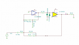
For fun I may have a small PC board fabbed with just a NJM2068 and a OPA551, then do my best with reactive loads to try to get it to oscillate.
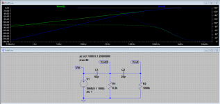
Also some small progress on the second order comp network. I was able to finally get my arms wrapped around this one from a post in the solid state forum right now, which I think may be similar to one of yours, from memory:
http://www.diyaudio.com/forums/solid-state/241799-two-pole-compensation-lme4702-lme49830.html
ImageShack® - Online Photo and Video Hosting
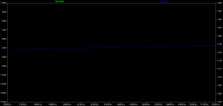
Feeding the network from the CC2 end I get 3dB down at 414kHz for the pole, plot below, exactly as advertised.
Thanks again for all your compensation ideas and suggestions!
Unrelated: if anyone has a pointer to measurements of organic solid polymer electrolytics' capacitance vs. voltage, please post or PM me. I'm always looking for reasonable alternatives to that expensive pile of WIMA 4.7uF film caps on each channel. Maybe nonpolar (back to back) solid polymers are a cheaper solution. I know that regular aluminum electrolytics have unacceptable nonlinear properties, but I don't think I've ever seen signal path measurements done with the new solid polymer caps, either aluminum or tantalum.
I've just spent some time Googling and searching on the forum for an OPA551 headamp with the chip wrapped in a linearization loop with some low noise, low distortion thing like a NJM2068 or LME49990. So far nothing, although I have found quite a few amps with just a straight OPA551 output from years back. I see that theAnonymous1 built one 6 years ago here:
http://www.diyaudio.com/forums/headphone-systems/95698-diy-headphone-amp-not-loud-enough-2.html
and the Violetric V90 uses them in the output stage
Violectric HPA V90 Reviews
which gave me a heads-up on something I missed, that chip has an operating voltage up to +/-30Vdc (60 volt swing!). Hmmm......
Now there would be an interesting "voltage select switch". Run that OPA551 output stage at a gain of 2x on +/-30Vdc rails so the driver circuitry could still be LME4990s running off +/-15Vdc rails. I have the place for the attenuator resistor in series with the volume control anyway, easy enough to cut the input in half if needed. I could easily generate +/-32Vdc supplies by switching in a couple of diodes and caps in the power supply to make a dual rail voltage quadrupler as opposed to the existing "O2" dual rail voltage doubler. I already posted that desgin in the mod thread sometime back. +/-15Vdc and +/-30Vdc would both be available at different tap points in the quadrulpler. A 60V swing should take care of every single high impedance headphone out there.
Also some interesting comments from NwAvGuy/RocketScientist during his chip tests with the OPA551:
NwAvGuy: O2 Design Process (search in there for OPA551)
For fun I may have a small PC board fabbed with just a NJM2068 and a OPA551, then do my best with reactive loads to try to get it to oscillate.
Also some small progress on the second order comp network. I was able to finally get my arms wrapped around this one from a post in the solid state forum right now, which I think may be similar to one of yours, from memory:
http://www.diyaudio.com/forums/solid-state/241799-two-pole-compensation-lme4702-lme49830.html
ImageShack® - Online Photo and Video Hosting
Feeding the network from the CC2 end I get 3dB down at 414kHz for the pole, plot below, exactly as advertised.
Thanks again for all your compensation ideas and suggestions!
Unrelated: if anyone has a pointer to measurements of organic solid polymer electrolytics' capacitance vs. voltage, please post or PM me. I'm always looking for reasonable alternatives to that expensive pile of WIMA 4.7uF film caps on each channel. Maybe nonpolar (back to back) solid polymers are a cheaper solution. I know that regular aluminum electrolytics have unacceptable nonlinear properties, but I don't think I've ever seen signal path measurements done with the new solid polymer caps, either aluminum or tantalum.
Attachments
Last edited:
- Home
- Amplifiers
- Headphone Systems
- A version of an O2 Desktop Amp (ODA)