Here are the Spice directives that I used :
.model 2N5457 NJF(Beta=1.125m Betatce=-.5 Rd=1 Rs=1 Lambda=2.3m Vto=-1.372
+ Vtotc=-2.5m Is=181.3f Isr=1.747p N=1 Nr=2 Xti=3 Alpha=2.543u
+ Vk=152.2 Cgd=4p M=.3114 Pb=.5 Fc=.5 Cgs=4.627p Kf=10.45E-18
+ Af=1)
.model 2N5460 PJF(Beta=1.107m Betatce=-.5 Rd=1 Rs=1 Lambda=20m Vto=-1.372
+ Vtotc=-2.5m Is=222.4f Isr=2.177p N=1 Nr=2 Xti=3 Alpha=29.8u
+ Vk=400.1 Cgd=2.34p M=.4822 Pb=1 Fc=.5 Cgs=2.92p Kf=673.9E-18
+ Af=1)
.model 2N5087 PNP(Is=6.734f Xti=3 Eg=1.11 Vaf=45.7 Bf=254.1 Ne=1.741
+ Ise=6.734f Ikf=.1962 Xtb=1.5 Br=2.683 Nc=2 Isc=0 Ikr=0 Rc=1.67
+ Cjc=6.2p Mjc=.301 Vjc=.75 Fc=.5 Cje=7.5p Mje=.2861 Vje=.75
+ Tr=10.1n Tf=467.8p Itf=.17 Vtf=5 Xtf=8 Rb=10)
.model 2N5088 NPN(Is=5.911f Xti=3 Eg=1.11 Vaf=62.37 Bf=1.122K Ne=1.394
+ Ise=5.911f Ikf=14.92m Xtb=1.5 Br=1.271 Nc=2 Isc=0 Ikr=0 Rc=1.61
+ Cjc=4.017p Mjc=.3174 Vjc=.75 Fc=.5 Cje=4.973p Mje=.4146 Vje=.75
+ Tr=4.673n Tf=821.7p Itf=.35 Vtf=4 Xtf=7 Rb=10)
.MODEL MJE200G npn
+IS=4.05292e-12 BF=380.795 NF=1.12262 VAF=3.13981
+IKF=2.93627 ISE=2.00947e-11 NE=1.68705 BR=0.235532
+NR=1.28142 VAR=2.69274 IKR=3.00157 ISC=5.4677e-13
+NC=3.93885 RB=3.97224 IRB=0.1 RBM=0.1
+RE=0.0001 RC=0.183575 XTB=0.1 XTI=1
+EG=1.05 CJE=2.005e-10 VJE=0.99 MJE=0.364577
+TF=1.51626e-09 XTF=1.18106 VTF=11.1354 ITF=0.00993068
+CJC=1.29309e-10 VJC=0.727072 MJC=0.261798 XCJC=0.8
+FC=0.565346 CJS=0 VJS=0.75 MJS=0.5
+TR=2.1444e-06 PTF=0 KF=0 AF=1
.MODEL MJE210G pnp
+IS=2.00939e-14 BF=239.361 NF=0.896718 VAF=25.7301
+IKF=7.3852 ISE=8.48474e-12 NE=3.31568 BR=3.52861
+NR=0.934743 VAR=1.2364 IKR=9.21648 ISC=1.75001e-13
+NC=4 RB=9.03053 IRB=0.0628113 RBM=0.098554
+RE=0.000934851 RC=0.199622 XTB=0.20806 XTI=1
+EG=1.05 CJE=1.48386e-10 VJE=1.38542 MJE=0.388741
+TF=1.42687e-09 XTF=1.19634 VTF=11.2194 ITF=0.00993432
+CJC=1.46449e-10 VJC=0.0628049 MJC=0.253896 XCJC=0.8
+FC=0.556255 CJS=0 VJS=0.75 MJS=0.5
+TR=2.58802e-07 PTF=0 KF=0 AF=1
Patrick
I used all resistor values as in the LA schematics, plus a resistive load of 60R.
Patrick
Next step would be to compare the SIM to measured data.
I assume you got it....when I mentioned stray C from pcb etc. It is pretty easy to get 10 and more pfd in practice.
Moving on, what is your SIM thd and we can compare that to my data shown back a few pages.
When all agrees with measured data you can tweek the SIM files to get the real world results to make a better SIM.
For your sim, you can show freq response at different Rload values.... in this type of topology, you can get different peaking levels with different load values.
THx-RNMarsh
I have not built.
Just curious how it performs.
This is what we build :
http://www.diyaudio.com/forums/head...ss-zgf-headphone-amplifier-2.html#post3372233
Patrick
Just curious how it performs.
This is what we build :
http://www.diyaudio.com/forums/head...ss-zgf-headphone-amplifier-2.html#post3372233
Patrick
Last edited:
I used all resistor values as in the LA schematics, plus a resistive load of 60R.
Yeah, me too. Checked it n-th time now, where n>>10...
Did you use the schematic from Figure 8 like I did? Or was it Figure 7? I just simulated Figure 7 and here 10pF are sufficient for me, too.
I received the JFETs from China today. Now I just have to find the time to match them properly. The weather is currently becoming great here, so I'll probably be outside for most of the day...
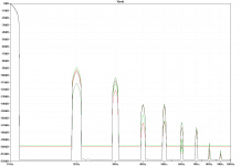
Here're some simulated THD results. Input level was 1.414V peak.
Green: Full circuit from Figure 8 with unity gain, 60R load, 2x47pF, EUVL's Models
Red: Same, but my models for substituted parts.
Dark Green: Buffer from Figure 7, 60R load, 2x10pF, EUVL's Models
Dark Red: Same, but my models for substituted parts.
Green: Full circuit from Figure 8 with unity gain, 60R load, 2x47pF, EUVL's Models
Red: Same, but my models for substituted parts.
Dark Green: Buffer from Figure 7, 60R load, 2x10pF, EUVL's Models
Dark Red: Same, but my models for substituted parts.
Attachments
Which device parameters are changed when you match devices and what results would you get with the use of the matched parameters in the transistor models?
That's a good question, and I'm still searching for an answer.
Unfortunately I'm no Spice Wizzard
 . I can do some stuff with LTSpice, but I have almost no clue of the models themselves.
Maybe I should read the corresponding chapters in the Tietze & Schenk, that might be helpful. Bad thing is, I can only digest it in small portions due to time constraints, which should make it a bit harder.
Which device parameters are changed when you match devices and what results would you get with the use of the matched parameters in the transistor models?
THx-RNMarsh
And, of course the follow up question will be - which parameters when matched will cause the distortion to be lowest.... then match devices for that/those parameter(s). And, use those matched parameters in the SIM files.
THx-RNMarsh
Never the less, you have respectable results with your SIM. Most people in HighEnd and DIY do use some matching as I did here to reduce distortion further than unmatched devices.... esp useful when the NFB is not high. BUT the SIM data is with models of complimentary devices which are Not matched. When matched, of course, the comp devices are more alike than your SIM uses.... your results are closer to what you will get with unmatched devices.
THx-RNMarsh
THx-RNMarsh
Last edited:
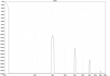
This time I used the full circuit and tweaked the output BJT's models to better match your k3 measurement. K2 can be lowered, but to achieve this I'll have to dig deeper into the FET models. Stay tuned .
The attached graph shows k2 and k3 over a load range of 30 to 300 Ohms.
.The attached graph shows k2 and k3 over a load range of 30 to 300 Ohms.
Attachments
Just finished measuring up all those 180 tiny little FET's. Tedious.... 
On a first look there're absolutely no matches. If Vgs(off) is about equal, then Id is way off and vice versa. Gfs is nicely separated between NJF and PJF with a huge gap in between.
Next up I'll try to tweak the models to closely resemble a couple of my measured results and then see which work best.
On a first look there're absolutely no matches. If Vgs(off) is about equal, then Id is way off and vice versa. Gfs is nicely separated between NJF and PJF with a huge gap in between
.Next up I'll try to tweak the models to closely resemble a couple of my measured results and then see which work best.
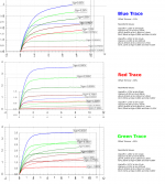
I arbitrarily picked three "complementary" pairs of my FETs and traced some curves. These were then used as the target to tweak the models using only three parameters. VTO was set to the measured value of Vgs(off), BETA was adjusted to match Id@Vgs=0V (this is the 'knee' where the curve traces start to run almost flat), and LAMBDA set the slope to match Id@Vgs=0V at about Vds=8V.
The first pair was picked for measured gfs, as good as it gets. The best PFET has 2.3mA/V while the worst NFET has 3.4mA/V. Total range was 1.8-4.2. This pair caused a huge DC offset, which was barely trimmable.
(Blue Trace)
Second pair was selected for a Vgs(off) of -1.70V, while the other parameters differed widely. This pair also caused a huge offset, albeit in the opposite direction.
(Red Trace)
The third pair was matched for a drain current Id of 3.50mA at the same Vds. DC offset was only marginal and easily trimmed out. A look at the measured curves below shows the overall best match of all this three pairs. It's still far from perfect though, cause all the other parameters don't match here, either.
(Green)
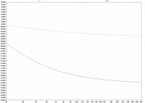
The first image shows an overlay of four simulation runs into 30 Ohms. The black trace is the result of using all standard models without any tweaks.
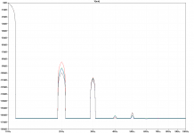
The second image shows the real world data of the used FETs. Please excuse the crude graphs; I simply stretched them to the same scale for easy comparison.
Note that the FET models were only rough estimates of the measured values. I'll probably try to create a nice overlay of measured and modeled data and then try to tweak the models further. The BJT models were tweaked already, albeit not perfect ideal matches.
The first pair was picked for measured gfs, as good as it gets
. The best PFET has 2.3mA/V while the worst NFET has 3.4mA/V. Total range was 1.8-4.2. This pair caused a huge DC offset, which was barely trimmable.(Blue Trace)
Second pair was selected for a Vgs(off) of -1.70V, while the other parameters differed widely. This pair also caused a huge offset, albeit in the opposite direction.
(Red Trace)
The third pair was matched for a drain current Id of 3.50mA at the same Vds. DC offset was only marginal and easily trimmed out. A look at the measured curves below shows the overall best match of all this three pairs. It's still far from perfect though, cause all the other parameters don't match here, either.
(Green)
The first image shows an overlay of four simulation runs into 30 Ohms. The black trace is the result of using all standard models without any tweaks.
The second image shows the real world data of the used FETs. Please excuse the crude graphs; I simply stretched them to the same scale for easy comparison.
Note that the FET models were only rough estimates of the measured values. I'll probably try to create a nice overlay of measured and modeled data and then try to tweak the models further. The BJT models were tweaked already, albeit not perfect ideal matches.
Attachments
Last edited:
The results just got a little worse .
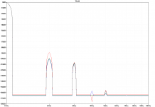
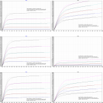
Spent some more time on creating graphs and on fine-tuning the FET models. This time I attached an image where you can find both the measured curves (all black traces) and the simulated curves (in color) for comparison. They're still not perfect and I didn't consider any dynamic parameters, but it should to the trick, I suppose. Notice that VTO is not equal to measured Vgs(off), but it's a good starting point.
This time, for the second set of curves (corresponding to the red trace), DC offset was ~20mV with the trimmer at full stop, so it can't be set to zero at all. Which leads to the conclusion that matching the FETs for Vgs(off) is bull.
On the THD side there's not much changed, except for k2 being about 5dB worse than before. Better models = worse results. Looks sound, doesn't it?
About making all that graphs:

(Thx to Mr. Munroe)
.Spent some more time on creating graphs and on fine-tuning the FET models. This time I attached an image where you can find both the measured curves (all black traces) and the simulated curves (in color) for comparison. They're still not perfect and I didn't consider any dynamic parameters, but it should to the trick, I suppose. Notice that VTO is not equal to measured Vgs(off), but it's a good starting point.
This time, for the second set of curves (corresponding to the red trace), DC offset was ~20mV with the trimmer at full stop, so it can't be set to zero at all. Which leads to the conclusion that matching the FETs for Vgs(off) is bull
.On the THD side there's not much changed, except for k2 being about 5dB worse than before. Better models = worse results. Looks sound, doesn't it
?About making all that graphs:
(Thx to Mr. Munroe)
Attachments
- Home
- Amplifiers
- Headphone Systems
- Marsh headphone amp from Linear Audio